AT25 Journal
This journal will document my findings and progress throughout the project.
Entry 1 (June 19th)
Time Spent: 3
Total Time on Project: 3
Day 1 involved researching and selecting the necessary components. I plan to order most of the parts from GreatHobbies, a Canadian hobby store.
Initially, I selected the battery based on my preferred voltage of 7.4V due to the availability of batteries and motors, and it being at an ideal performance range. For the capacity, I opted for 5000mAh to achieve a decent runtime while remaining cost-effective.
Next, I chose the motor, which required thorough research and consideration. After evaluating the options, I decideed that using a single motor for a RWD setup would offer better cost-effectiveness and performance than 2 motor AWD. The selected motor is a 1406-2280KV, 4-pole sensored model, which can be found in the Bill of Materials (BOM).
Lastly, I selected the tires. Although I originally wanted RC slick tires, the best available option was vintage racing tires. I chose a 26mm width for the front tires and a wider 31mm for the rear.
The BOM can be found at the following link: AT25 BOM

Entry 2 (June 20th)
Time Spent: 2
Total Time on Project: 5
Today, I began laying out the general design of the car. I began by learning how the aerodynamic elements work and the different elements used. Through this, I got refreshed on Bernoulli's and got a surface level understanding on how the important elements work.
Knowing this, I made a rough sketch on paper as a guideline on how I will design the car. This rough work can be found below.
Finally, I made and found the 3D models for the components I will be using. My plan is to design the aero then determine the packaging for everything else, a similar process used in F1 and other design teams.
Note: I changed the battery to a different, similar spec'd one due to a proprietary connector.

Entry 3 (June 21st)
Time Spent: 5
Total Time on Project: 10
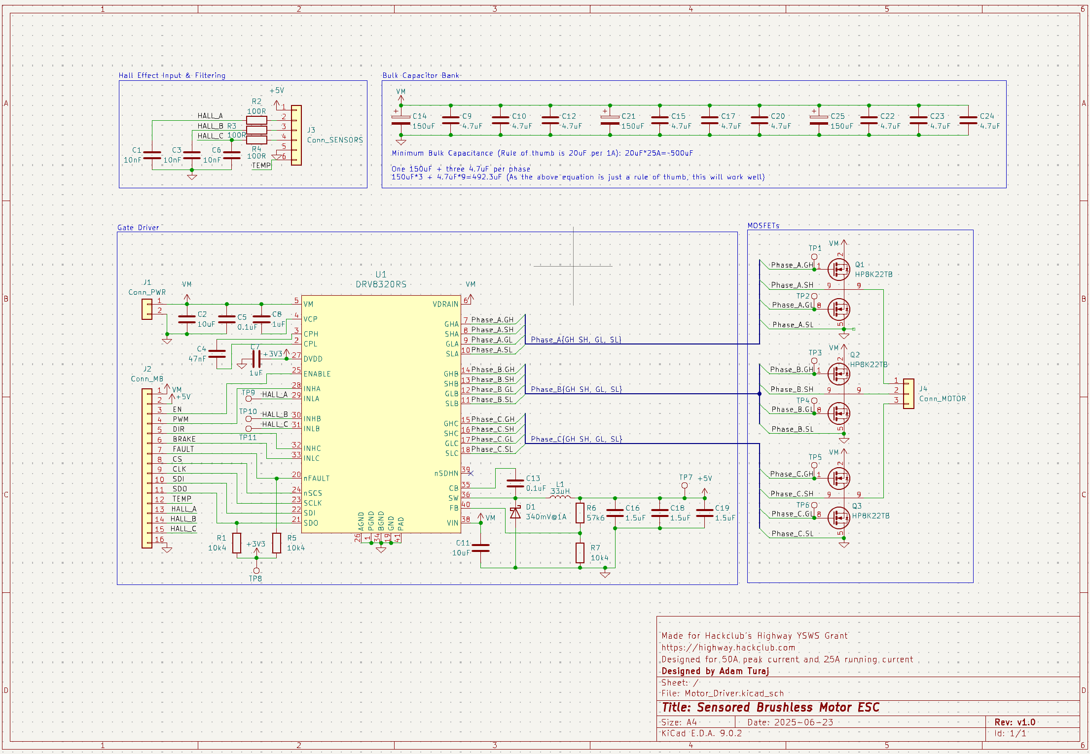
In Day 3, I began work on the brushless control board. The IC pre-driver I selected was the DRV8323S due to its 1 PWM mode (no extra code required), my previous experience with it, and its availability.
I preferably would run the DRV8320S but it is out of stock so I had to compromise. This IC would be better as it doesn't include the amplifiers which are not required due to the sensored motors not needing to know the current flowing through the coils.
Afterwards, I chose the CSD87333Q3D FETs as it is TI (I love Texas Instruments), it integrates both the high and low MOSFETs, supports up to 15A (the limit I'm designing for), and the high efficiency while being cheap and available.
Drawing the schematic mainly involved following the diagrams provided by TI. It was very straightforward; however, the PCB layout will not.
The final schematic for the board is this:

Entry 4 (June 22nd)
Time Spent: 3
Total Time on Project: 13
I did some more research while looking for footprints and came to the following conclusions:
- I will be attempting to assemble the boards myself again
- Bulk capacitor banks are required
- The DRV8320RS is preferred for my application as:
- I do not need the current sense amplifiers (I'm using a sensored motor)
- The buck converter is necessary for my application
Regarding conclusion #1, I will be assembling them myself due to the high costs of JLCPCB assembly, and my previous experience assembling SMD boards. I had issues assembling my last board which is the reason I was planning on using PCBA; however, I made the realization that my solder paste is expired which I believe is the source of the problems.
After making these conclusions, I adjusted my schematic to reflect them. This included updating the DRV footprint (although I haven't changed the pinout from the DRV8323RS -> DRV8320RS). The capacitance of the bulk bank was stolen from an existing open source design.
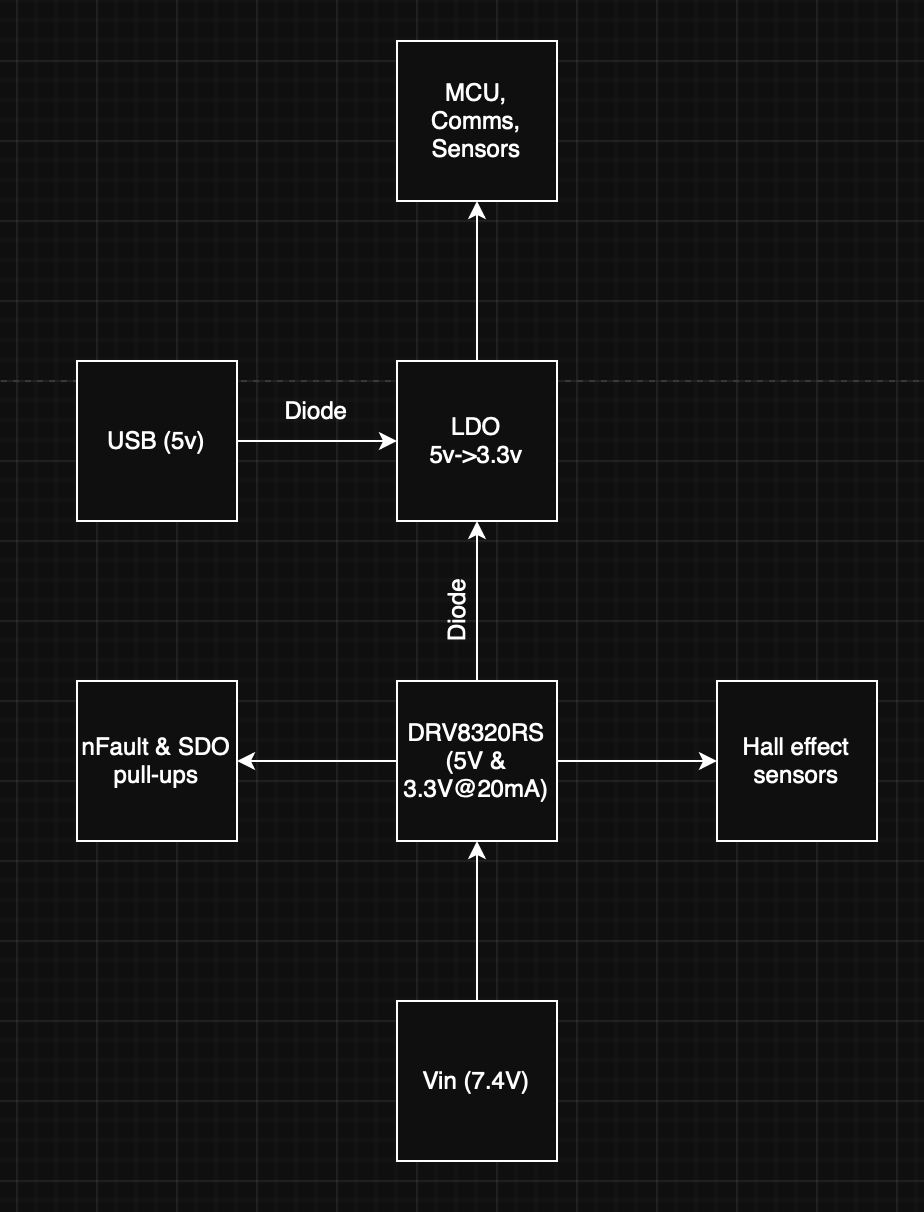
I started adding the circuitry around the buck converter but still need to fill in the values. Below is my plan on how the board will be powered:
And here is the current revision of the schematic:
Entry 5 (June 27th)
Time Spent: 7
Total Time on Project: 19
Throughout today, I tweaked the schematic, picked parts, and designed the layout.
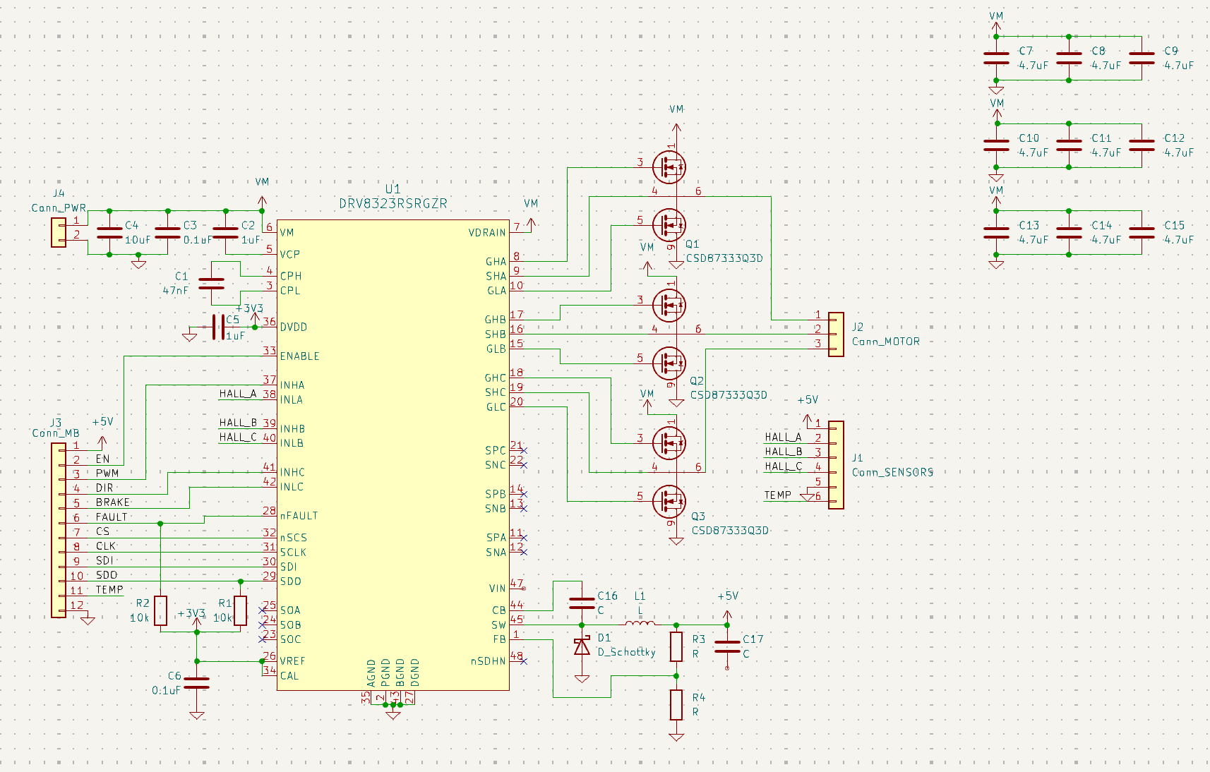
Firstly, I made the following changes to the schematic:
- Added a RC filter to the hall effect sensors
- Adjusted the symbol to the DRV8320RS
- Finished buck converter circuitry
- Change 10uF bulk capacitor to 100uF electrolyte capacitor
- Added 0.1uF capacitors to each gate
- Cosmetic adjustments
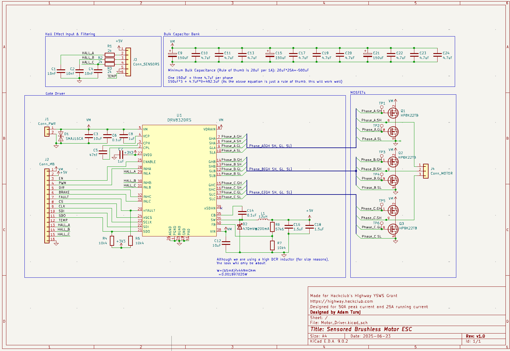
These changes resulted in the final, completed schematic:
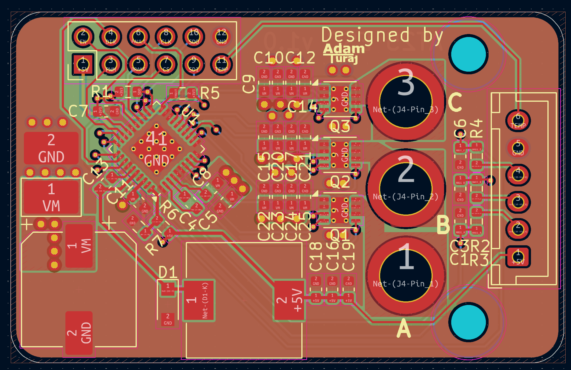
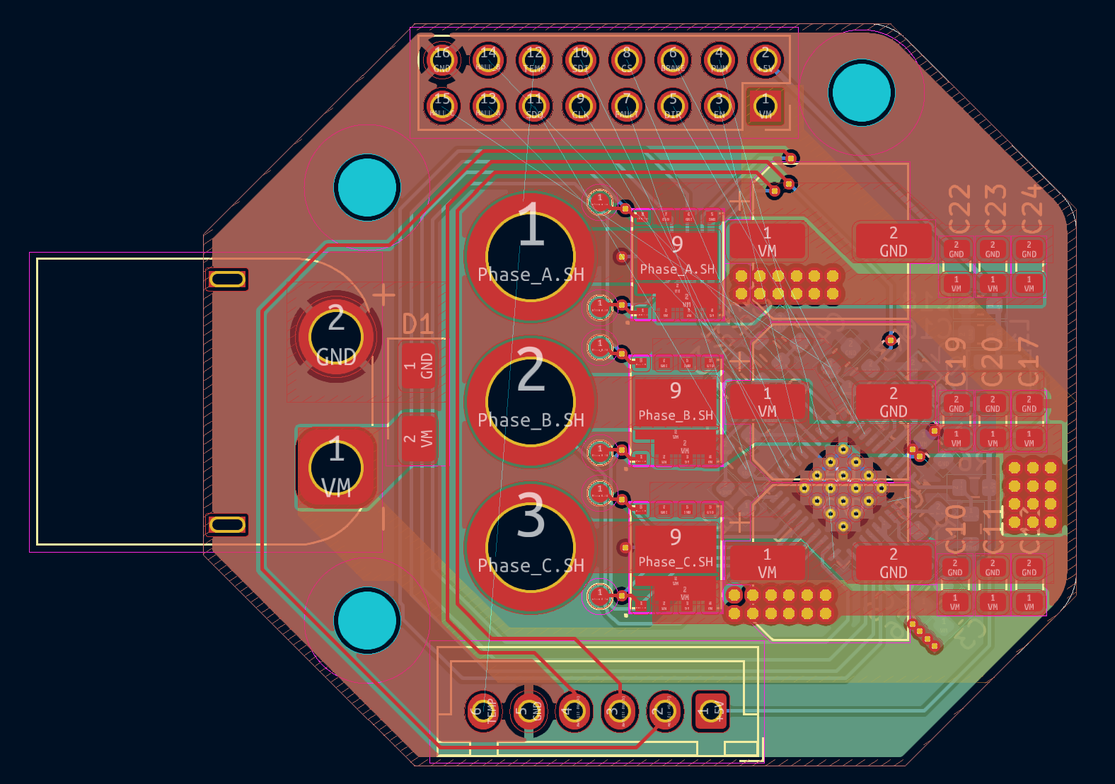
Afterwards, I assigned footprints and picked part numbers. With all that done, I layed them out, and carefully wired them up. Due to the relatively high current and to simplify wiring, a 4 layer board was a no brainer. The stackup I used, as I have done with all my other 4 layer boards, is:
- Sig / GND
- GND
- PWR
- Sig / GND
For the first time ever, I made the entire board without a single DRC error: no clearence violations, missed connections, etc!
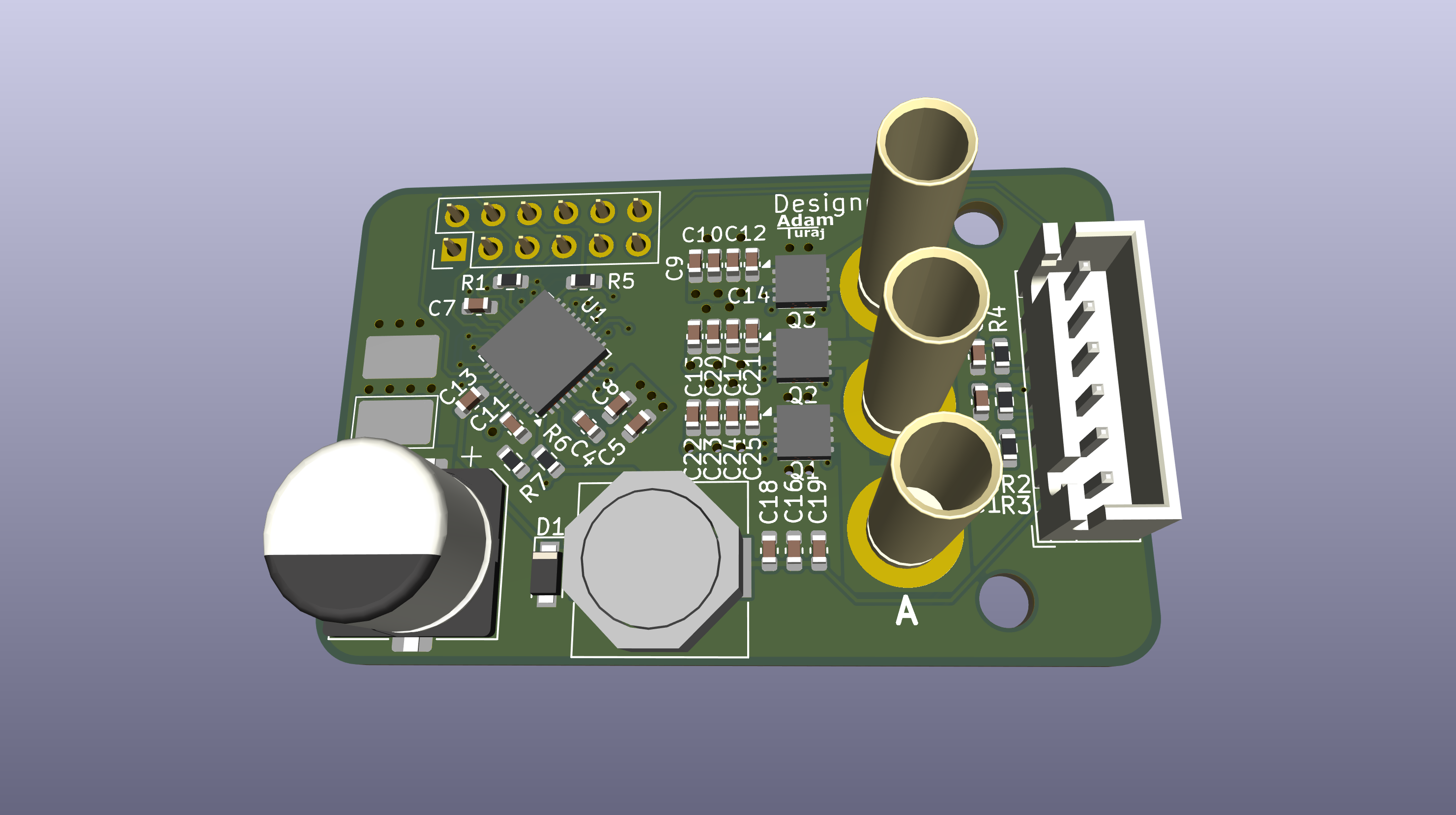
Below is the final design for the ESC:
Entry 6 (July 2nd)
Time Spent: 5
Total Time on Project: 24
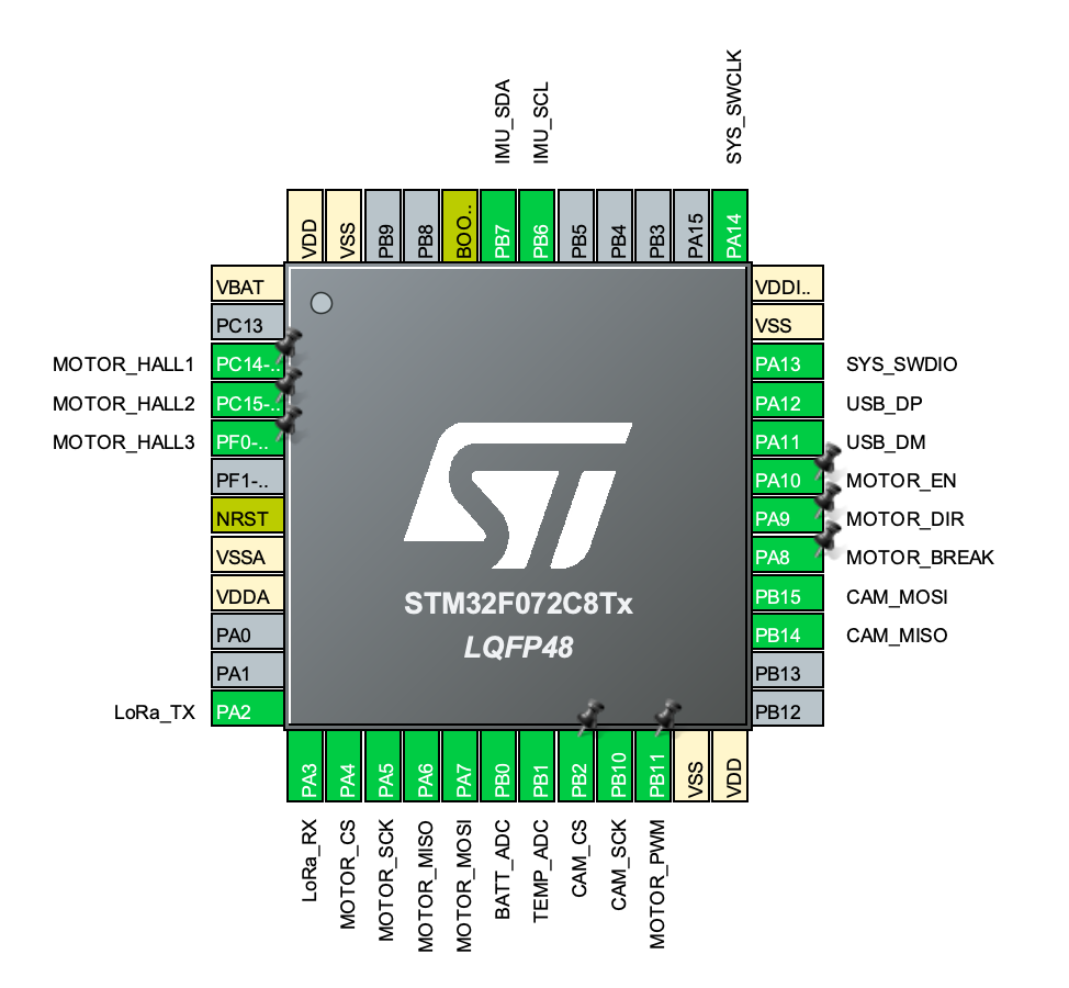
I began by starting the motherboard. This first involved picking the MCU which I chose to be the STM32F072. I chose it due to its small form factor (48 pins), availability, price, and it supporting all the peripherals I needed.
Afterwards, I assigned all the pins in the STM32CubeMX. I assigned:
- SWD
- USB
- DRV8320 pins (SPI + PWM, DIR, and BREAK)
- Camera SPI (for the future)
- LoRa UART
- IMU I2C
- Battery and Temperature ADC's
- The three hall effect sensors inputs
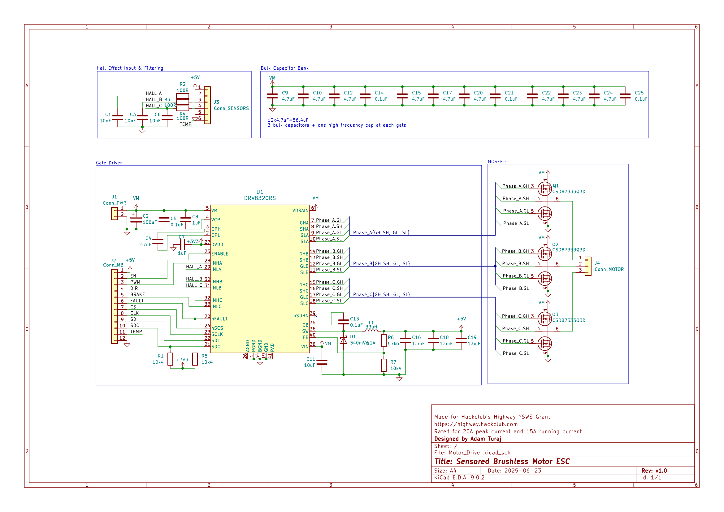
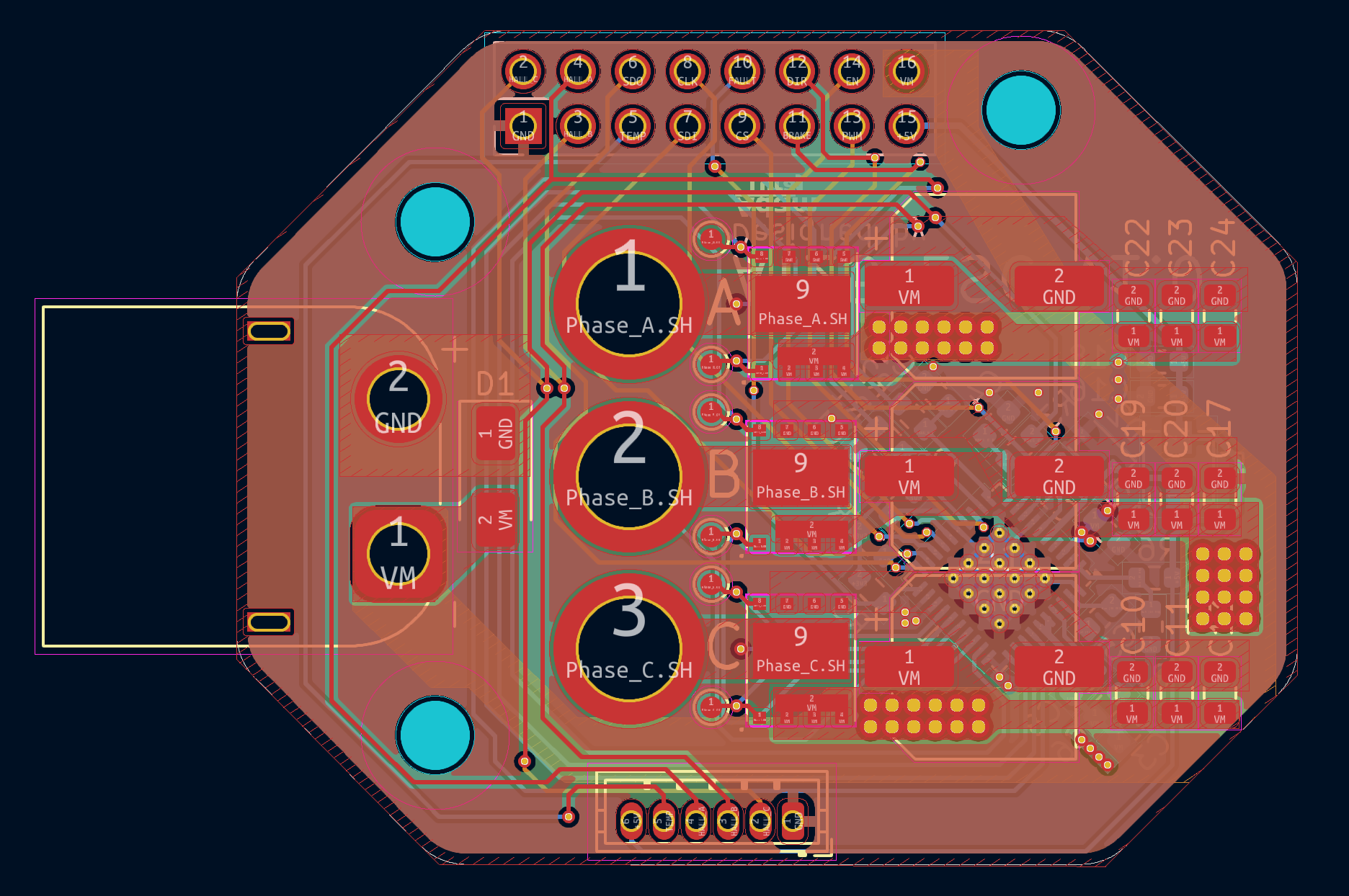
While assigning the pins, I fell down a rabbit hole which led to me redesigning the ESC control board to accomodate more current (25A continuous instead of 15A), adjust the bulk capacitors, and improve the routing.
I found this really good article from Alexander Sysoev on Zubax which helped me pick the bulk capacitors, make sure the new MOSFET is sufficient for my use casee, and improve the routing.
Here is the updated ESC schematic:
Entry 7 (July 3rd-5th)
Time Spent: 6
Total Time on Project: 30
After some minor adjustments to the schematic, I assigned footprints and part numbers to the new components. Afterwards, I began laying everything out.
I am considering using a 6 layer board; however, I do not think that will be necessary. After laying out the important, high current lines using large ground pours, I began tracing the signal lines which was more of a puzzle over anything.
Anyways, below is the current schematic and PCB at the time of the commit:
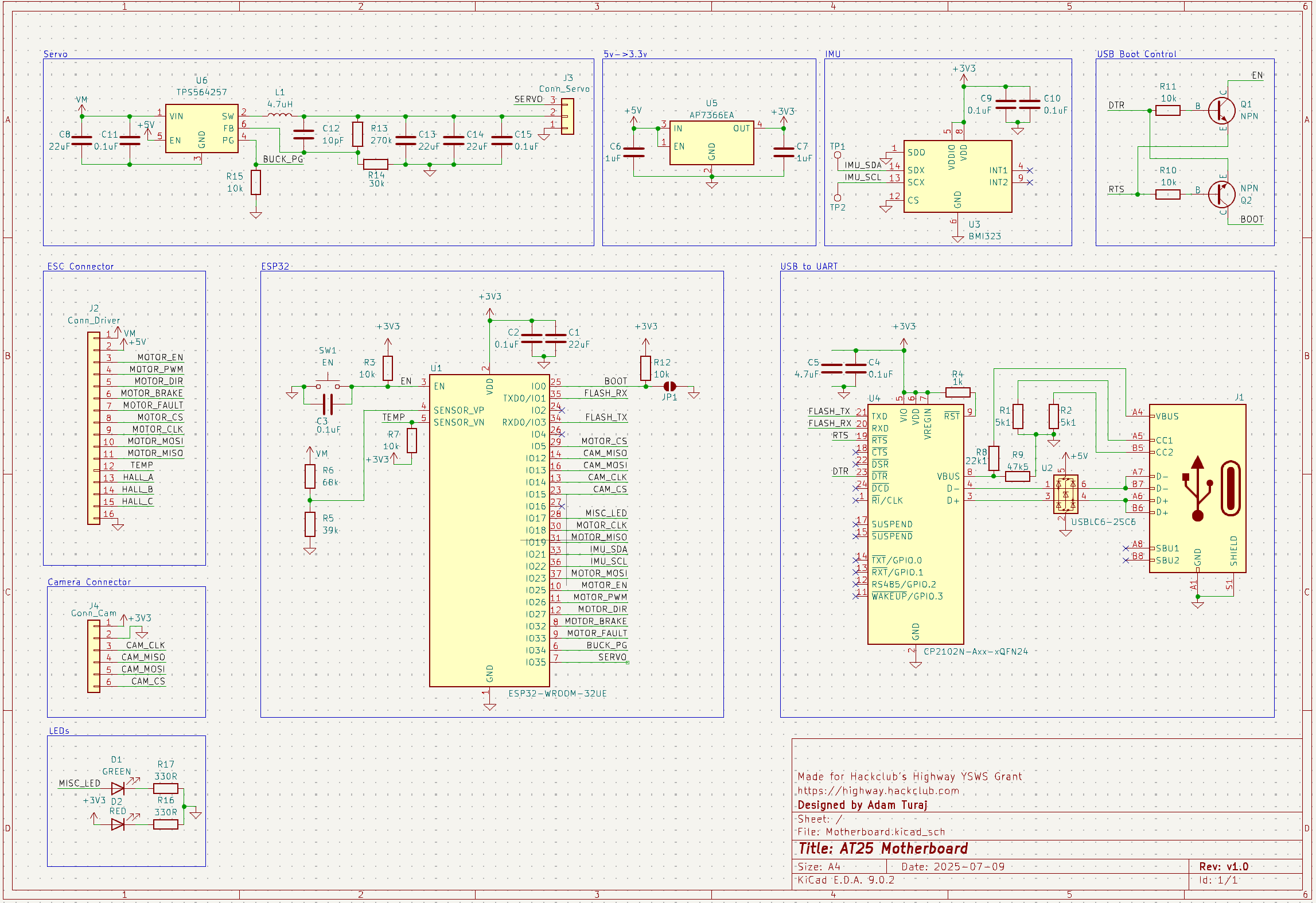
Entry 8 (July 6th, 7th & 9th)
Time Spent: 8
Total Time on Project: 38
Over the three days, I finished the schematic for the motherboard and the motor driver layout.
I was able to route the motor driver using only 4 layers. It required some rejigging of the hall effect traces. I also beefed up the buck converter circuit to a 600mA max current to accomodate the camera and a change to the MCU (which I will talk about soon). Afterwards, I carefully routed all the signal pins being mindful of VM.
This resulted in the following PCB:
Next up was the motherboard. While researching using the SX1280, I ran across the idea of using an ESP32. Due to wanting to use a camera, and range not being super important, an ESP32 would be a better choice over the slower, but longer range SX1280.
I landed on using the ESP32-WROOM-32UE-N4 so I can use an external antenna (for longer range), and to ensure I have enough pins and processing power.
I first wired up the MCU. This involved adding the decoupling capacitors, adding the reset button, and wiring all the peripherals and pins needed for the motor driver. Next, I added the IMU and wired all that up to the datasheets spec. The IMU was chosen based on it being the cheapest.
Then, I setup the UART to USB converter. Due to there being no native USB flashing support, the circuit is required. I went with the CP2102N due to it being commonly used on other PCBs. The RST and BOOT circuitry at the top right was ripped out of the official devboard of this chip.
Afterwards, I dealt with the power. I quickly wired up the LDO which will drop the 5v -> 3.3v. The servo will require its own buck converter as the one builtin to DRV8320 is too weak. I went with a TI DC-DC converter as they have a really powerful circuit calculator making the designing the surrounding circuitry much easier.
Below is the current revision of the schematic: