
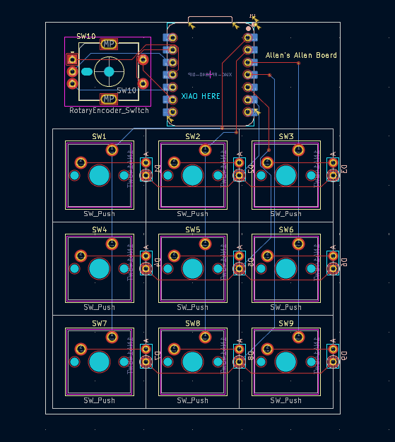
May 31: Making the Schematics
Hi! this is my first ever hardware project, and although I don't believe Journaling is mandatory I thought it best to document everything. Finally installed OPL Kicad Library after 30 minutes, hopefully the entire process isnt this slow. For my schematic How to design Mechanical Keyboards PCBs with Kicad was very helpful
I knew how I wanted my macropad to look like, and after copying the HackClub tutorial exactly I decided to try again but this time creating a matrix
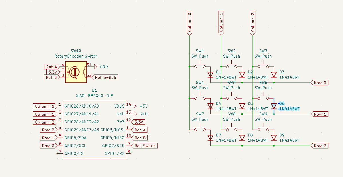
Honestly can say the hardest part of this was trying to find the correct footprint for the parts but I'm happy with what I learnt Total time spent: 2H30min
May 31: Completing the PCB
At this point, I had to stop relying on tutorials and start problem solving on my own. Many things came up, especially when routing the traces. I accidently moved the MCU then saved and closed Kicad, so wouldn't recommend as I had to reroute lots of things.
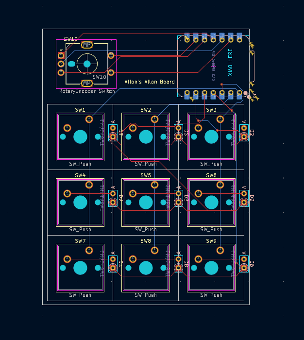
Total time spent 2H
May 32: Beginning the case
So I started off thinking that the case would be one of the easier steps of my process, but how wrong I was.
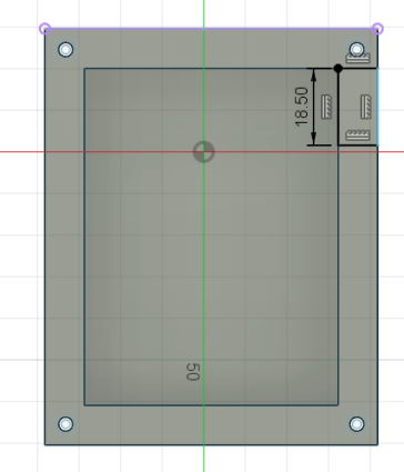
Turns out my schematics woulddn't fit properly with the case, based off where I put the MCU and how it lined up with the holes. I could either redesign the case, or fix the PCB which I figured would be better as to not create further problems later on.
Total time spent 2H
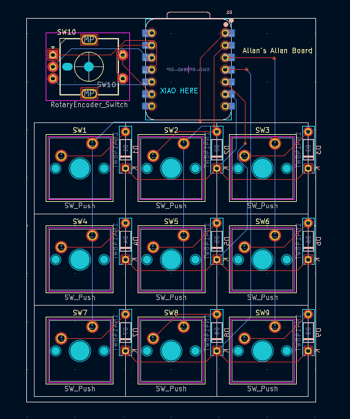
May 32: Refinishing the PCB
Initially It was going well, I rerouted the traces connected to the MCU, like 10 of them.
Yeah so turns out I made the same mistake again I only rotated the MCU, instead of centering it to avoid interference with the case. Time to redo again. also note: I actually made the biggest mistake ever I closed the window for some reason so I couldn't just revert my changes.
Finally finished, I made sure to double check that nothing was going to interfere. On the brightside, I learned a lot about routing traces, and I made sure to be more careful as I know If there was mistake I have to correct it.
Total time spent 45min
May 32: Finishing the CAD
Mostly just working on it, not much to say
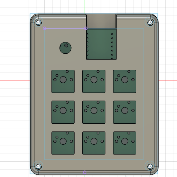
Total time spent 2h
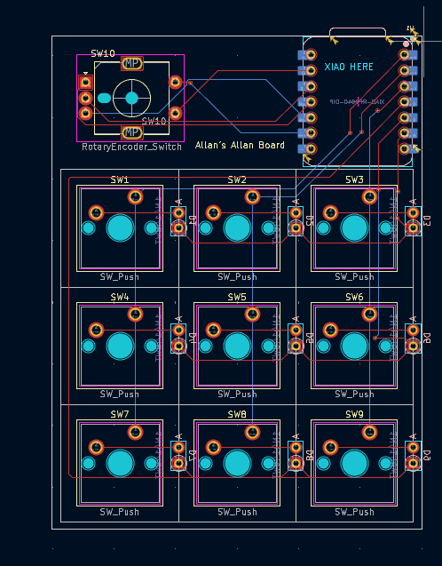
June 4: fixing my pcb
Kind of odd, I got my project approved (please don't unapprove) then I go on hackpad website, I used the wrong diode footprint Actually easier fix than I thought, I thankfully only had to reroute a few easy traces, and it doesn't impact any functions.
pictureeee
My gerber file for the pcb manufactuer finally got accepted after like 3 times so that's also cool also just realised half of my journal entries are may 32 so lots of fun
Total time spent 20min