
glyph
[ a custom split keyboard for portably and comfortably interfacing with computer systems ]
[hours spent so far: 19.5]
[ JOURNAL_ ]
[ MAY 27: IDEA ]
Hello world! I'm working on Glyph, a fun, portable, and comfortable split keyboard. It's the logical next step after designing and fixing the Hexapad. In this session I mostly just worked on the layout and gimmick of the keyboard. The key assignment isn't done yet but I want to start on the PCB now so I'll save that for later. Glyph has a finger-staggered main matrix of 6x3, and a key and joystick for each thumb. The joystick is the main gimmick of the board - you'll use it to switch layers and navigate documents. I started designing in FigJam but realized it would be hard to match up with my hands so I moved to using my notebook instead. While the keymap isn't complete, I'd like to have a layer for symbols, specials, and metas. Symbols include the number row and misc symbols like +, - and =. Specials - accessible with the right thumb - are brackets, quotation marks, /, and other common programming symbols. Meta keys are keys that adjust the keyboard, like RGB.
[hours worked this session: 1]
[total: 1]
[ MAY 29: BASICS ]
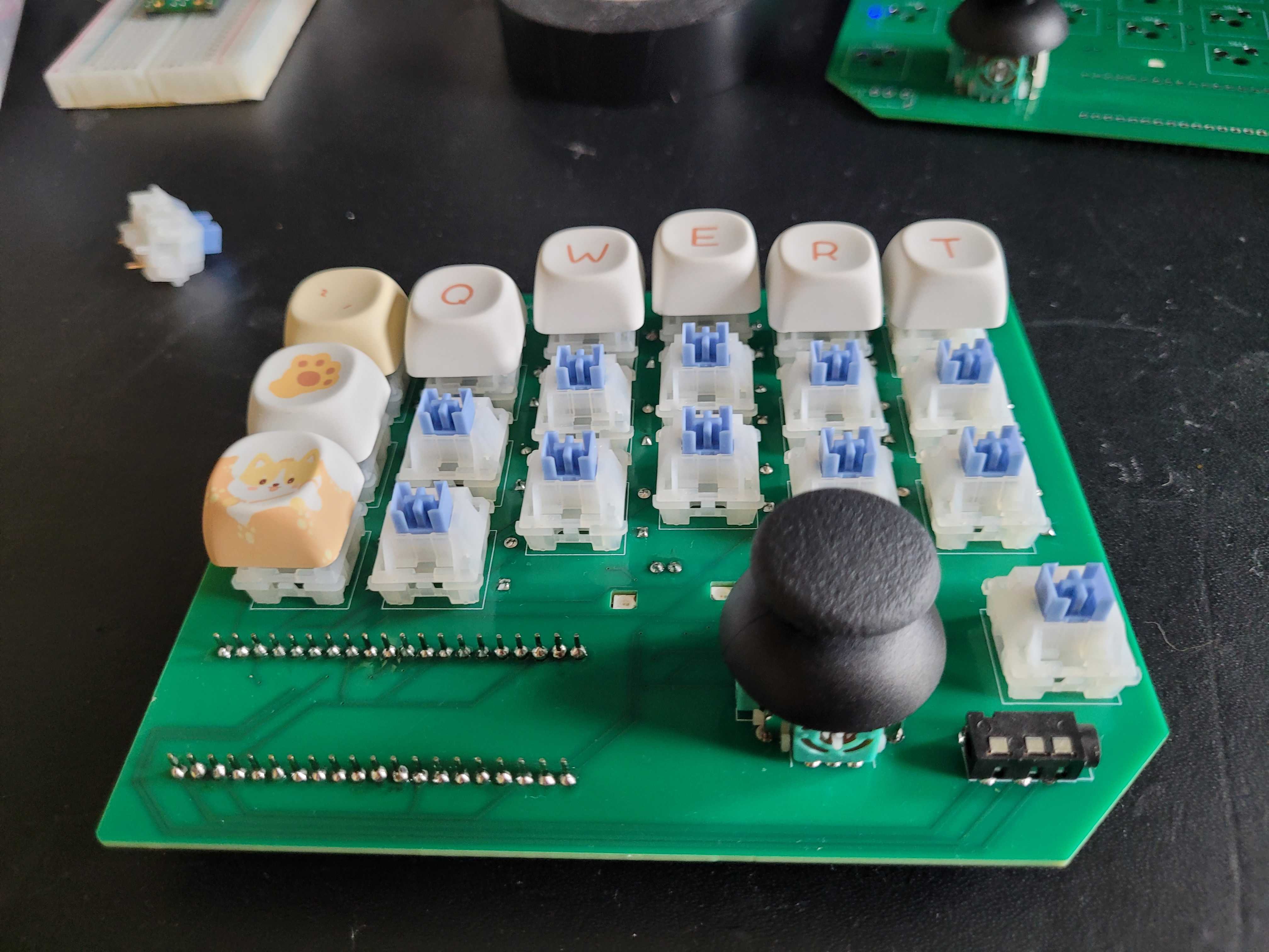
Hey again! Today I'm going to be working on the basic skeleton of the left half of the keyboard. In my spare time I've been trying to find a suitable joystick - first googling around for one I found on Adafruit (this one), then realizing SnapMagic exists and searching there. I eventually settled on the COM-09032. I then spent a LONG time trying to figure out how to get the symbol and footprint into KiCad from SnapMagic. After trying a bunch of different things (turns out there IS a kicad plugin but it's for an ancient version) I figured out how to import a footprint and started on design.
For glyph I'm going to be using a Raspberry Pi Pico - I have a bunch of them and they have plenty of I/O and are easy to work with. After spending a fair bit finding a reference for the matrix (ended up taking a screenshot of the Hexapad's matrix and using that) I got to work popping the switches down!
This was mostly just copying and pasting. Then I researched how to use a joystick with Pico, and after tracking down a broken link on SparkFun's product page, arrived at this wiring:
(side note: the sparkfun product page included an explanation of how the joystick worked, which i found super neat)
And to finish today off, I quickly added the thumb button:
Tomorrow (which is friday :yay:) I'll add the RGB and start on the PCB design - hopefully I can knock out the entire PCB this weekend and only need to finish the case and firmware!
[hours worked this session: 2]
[total: 3]
[ MAY 31 // GLOW ]
[note: I forgot to save while writing this so I'm rewriting this entry from memory on Jun 2]
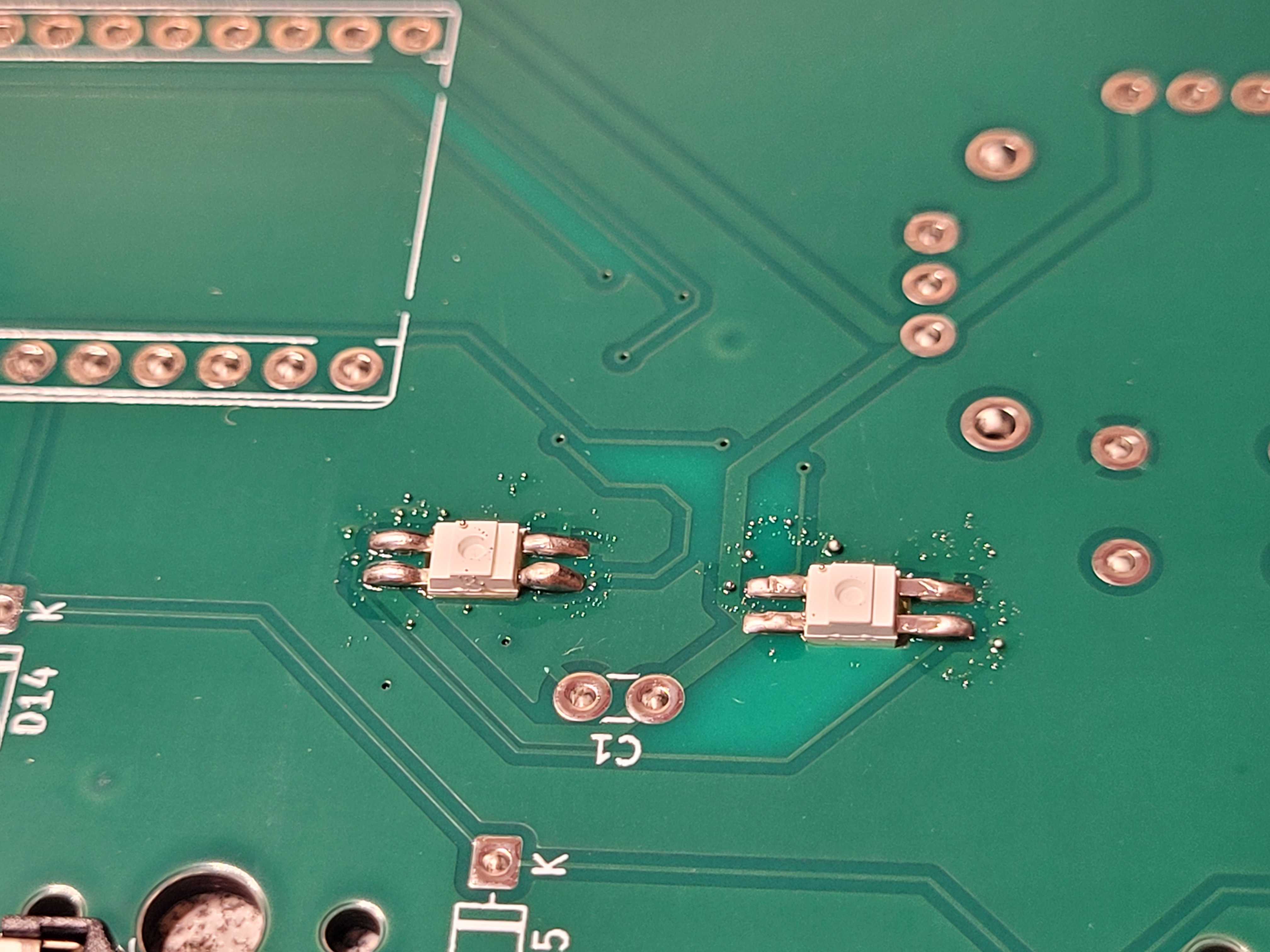
Hai :3! Today I'll add the RGB and start on the case design. I started researching different NeoPixel-style LEDs - I wanted something small but still reasonably hand-solderable. Instead of doing perkey RGB, which takes a lot of resources and a lot of soldering, I'm going to do something like an underglow
with 6 RGB LEDs on each side. However, the Adafruit docs say you need a 0.1uF capacitor for each neopixel, which was pretty annoying for the Hexapad. But the docs also say in some cases you can do 1 cap to 2 LEDs, knocking it down to 3 caps per side, which I'm comfortable with. I googled around (these ones were pretty common but looked hard to solder), and eventually found these NeoPixels with nice, long legs that should be good for hand-soldering. Turns out these are actually the reverse-mount LEDs people were using for their hackpads! After debugging a weird KiCad crash (and it magically working again 🙄) I imported the ScottoKeebs library and had a slight struggle wiring up the neopixels with 1 cap per pair. Some digging made why the cap was needed click
and I found that I was doing it all wrong. Here's the final, corrected wiring I ended up with:
To finish off today I assigned all the footprints (using hotswaps for the switches) and moved to the PCB editor.
[hours worked this session: 1]
[total: 4]
[ JUN 4 // ARRANGEMENTS ]
[ done in the Highway Roadtrip call! ]
I was just about to start laying out the PCB, when I realized... the PCB needs a way to talk to the other half of the keyboard. After some googling around I came across a Reddit thread suggesting UART, which doesn't need pullup resistors. Nice! This also fits perfectly with a TRRS jack (power, tx, rx, and gnd), so I used the ScottoKeebs TRRS symbol.
I put it in to the Kicad PCB editor and struggled to setup the grid properly so I could lay out the keyswitches. After (eventually) fixing the snapping settings to make it work I started laying down the switches:
... and promptly realized I wasn't doing them in the correct order. Quickly fixing them (it was actually quite relaxing), here it is:
I then added the diodes (KiCad crashed while doing this! Scary! But luckily it autosaved my work and I didn't lose much), and arranged the other parts. The RGB is in three corners and I found a lovely spot for the Pico and TRRS jack.
That's all for today! Tomorrow I'll route the whole thing (!!), print it out to test for fit, and get to work on the right side.
[hours worked this session: 1.5]
[total: 5.5]
[ JUN 9 // ROUTING ]
Hello!
I booted up Kicad and started getting ready for routing. First, I noticed that the hotswap sockets... were on the back of the PCB? That didn't look right. But after some googling I found that these actually were supposed to go on the back of the board. As well during my research, I found that millmax 0305s were a pretty popular hotswap option, but ended up deciding against them because it would mean a lot more soldering. Flipping all the components to the sides they were supposed to be on, I assigned 3D models to some of the parts:
On to routing! This time for Glyph I'm going to manually route everything because when I used an autorouter for the Hexapad it produced some... interesting results. Some searching around on Reddit produced this thread which suggested some track widths I'm comfortable with. I'm also going to try a ground pour with Glyph, which should make routing a little less painful.
I also edited some footprints to make them easier to solder:
When I started routing I realized I still needed to print out the PCB to check for fit. But my printer was out of ink, so I did what any normal person would do, and taped a piece of paper to my screen and traced out all the keys.
After painstakingly replicating my layout, I checked it against my hand and it was pretty comfy! So I switched back to routing.
There isn't really much to say about this other than that it was very relaxing.
Chonky 3v3 lines for the LEDs:
With only a few routes left, I ran DRC and got this strange hole clearance error. The ScottoKeebs footprint put a NPTH REALLY close to the pin hole. Weird. I spent a lot of time trying a lot of different things and ended up removing the board-wide clearance for copper-to-hole. The netclass still has a 0.2mm clearance and this allows the footprint's clearance override (which I'm assuming is to fix this problem) to take effect.
There were a few more DRC track clearance errors, so I fixed those up. Some clearance-fixing and routing later, Glyph[Left] v0 is done! Apart from the PCB art and outline, of course.
[hours worked this session: 2]
[total: 7.5]
[ JUN 14 // REPLICATION ]
Today I'm going to finish both sides of the PCB! This includes the PCB art, and then completely duplicating and flipping the design.
I started up Figma and did some light finagling to get to this:
On the PCB:
I then duplicated the left folder and renamed everything, and started rearranging the right side PCB to match my sketch. During a quick break, it occured to me that I should make sure that my keyboard switches match a 1u grid. I know I tried to do this back when I was laying them out, but KiCad grids are hard.
Checking each switch with the Ruler tool, I noticed one particular one that was a teensy bit off. I spent WAY too long fiddling with KiCad's snapping settings trying to get this to move, but eventually I lined it back up again.
Turns out this was a VERY good idea! A lot of other switches were off by a little bit. I also made the thumb switch match the grid. I duplicated the left project once again, and started my rearrangement.
Now, to reroute the whole right side. Luckily I had a pretty good idea of what to do here (what order, trace widths, etc) so it went quicker than last time.
I used a LOT of vias, but after a bunch of routing, I got to 0 DRC errors. Amazing!
Updating the silkscreen art, here's the full right side:
That concludes the PCB section of this journal! Now onto the case. I use OnShape for CAD, so I started a new project (with tabs for the left and right sides). I then hopped into Keyboard Layout Editor to try and replicate my design. Here it is for the left side :3
That's all for today! Glyph is getting closer to fruition. All that's left is the case and firmware. See you then!
[hours worked this session: 2.5]
[total: 10]
[ JUN 20 // MICRO ]
Hey again! Today i'm going to try to finish both cases. Then I'll be ready for firmware tomorrow and submission the day after.
To start this session off, I exported the left-side PCB and tried to put it into OnShape. The file was really complex and slowed down the website a lot, so I had to re-export in KiCad with some settings disabled. A lot of settings-tweaking later, I ended up compositing the PCB model in its own tab and deriving that in my main tab.
I got a plate from the ai03 plate generator and dropped it into an Assembly with the PCB. Checking for fit, I noticed that I had messed up some of the switch positions in KLE! I edited that, reimported, and got here:
In the cross-section view you can see that there's no spot for the joystick, which isn't good! Like the Hexapad, I'm doing a sandwich mount minus the top frame, which means I need to make a hole for the joystick. I quickly added that and spent a while fighting OnShape about which point to move after editing a dimension, I managed to make the plate a little smaller:
Some more dimensioning and cutting brought me to this. I also made the cutout for the joystick a hexagon, which I think looks really cool. I'll probably have that hexagon extend into the full case. However, I have to think about how I'm going to fit everything else - namely the Pico, RGB and TRRS jack, into the case.
Alright, so due to a lot of interruptions I didn't have much time today, but I think I'll be able to finish the case tomorrow, firmware on Sunday, and submit on Monday. Let's see how that goes. You can find my OnShape design here, I'll add it to the readme later.
[hours worked this session: 0.5]
[total: 10.5]
[ JUN 21 // MODEL ]
I was thinking about Glyph last night, and remembered that I needed to change the power circuitry for the right side. Right now power goes to VBUS, which can work but will explode if ever connected to USB. Not good! I booted up kicad once more to update that schematic and PCB. Luckily this was a fairly easy change since the VBUS and VSYS pins are right next to each other on the Pico. I then switched back to OnShape to continue on the case. Extending the hexagon shape and outlining the case, I started to build up the other parts and sides:
When making the walls, I needed to check how tall they should be to fit the Pico. For some reason KiCad didn't include a 3D model of the Pi Pico, so I set out to find one on GrabCAD, and got this one. I had to sign up for an account to download (why the hack do you need my phone number????), but eventually got it into my main assembly in OnShape. Some light translation got me here:
I then quickly added the bottom of the case, and then set my sights on the USB hole and TRRS hole. Sadly, the TRRS hole will have to go through the hexagon cutout (which looks ugly) because the jack is too tall. My CAD software produced some... unique results:
To finish up today, I cleaned up the case a little and made the bottom side smaller so the hexagon pattern could stick out more.
That's all! I didn't get as much as I wanted to done, but I think I'll be able to get the case and basic firmware done on Sunday.
[hours worked this session: 1.5]
[total: 12]
[ JUN 22 // ALMOST ]
Screw holes!
I was missing screw holes in my case. But before I fixed that, I tweaked some dimensions in the sketch to make the hexagon more prounounced. I then turned to the screw holes. I already have some M4 nuts and bolts from the Hexapad, so I tried to find their specs. The hole itself was quite easy - M4 means 4mm. But I had to do a lot more digging to find the specs for my nut, and ended up on this ISO specs page
Holding the nuts up to a ruler (because i don't have callipers :noo:), it looked like they were 3mm tall and 7mm from flat-to-flat, which matches up with the min/maxes on the table. I fought OnShape to expand the walls (it's probably just my terrible sketching skills) and sketch the holes:
I also split the case into two and connected them together with OnShape's very nice mate system. Next up is the USB hole. I did this the same way I did for the Hexapad - creating a new sketch with a rectangle, and using a remove extrude to cut out a hole. It felt quite refreshing to work in a sketch that wasn't the absolute mess of my plate!
Originally I was going do to something similar to the Hexapad, with outset text on top:
But I think this time I'll put the text on the sides. It looks way cooler and sleeker:
While I was doing this I had to figure out how to flip a sketch (I was drawing on the left side and my plane was the right plane.), and learnt that sketches could use mate connectors as planes. I flipped a mateconnector until the sketch was correctly oriented, and ended up with this really nice effect!
Now onto filleting. While filleting the top plate I misclicked and selected a face instead of an edge, producing a pillowy
effect I'm quite fond of. However, when I tried to apply this to the entire thing, I ran into a fillet error on one of the sides. This side, for whatever reason during my terrible sketching, was two faces split by an edge. Some research led me to the delete face
tool, which worked perfectly and allowed me to finish this really neat touch:
I then filleted out everything else, and the left-side case is done!
Onto the right case. I wanted to see if I could be lazy and just flip my left design and tweak a few positions, so I imported the right PCB and duplicated my Part Studio, deleting everything except the sketch and mirroring it. If this flip works, and there are no major changes that need to be made, it would save me hours.
It frickin' worked.
I re-extruded and tweaked some sizes to fit the slightly different part locations on the new PCB, then tried to add more clearance for the top and right sides, which the board was clipping into. The top side worked easily but I had to (yet again) fight my CAD software to let me re-dimension the right side. It was very annoying but I did learn about driven (like a ruler) and driving (forces the sketch to change) dimensions. No need for a USB port on this side, so I skipped to the text inset:
To finish up the case, I filleted everything up:
And that's it for the Glyph case!
This was a huge entry, but Glyph is almost done. I can see the light at the end of the tunnel.
Firmware's up next.
[hours worked this session: 3]
[total: 15]
[ JUN 25 // FINALITY (?) ]
School's out!
I'm hoping to submit today. Flights to Undercity are getting expensive and review takes 3-4 days, so I need to lock in. Before the firmware, though, I needed a basic layout. After cleaning my hideous (🫣) desk, I opened my notebook back up and tweaked the layout from the first entry.
Now onto which firmware to use. Joysticks aren't very common on keyboards so I need something that's either really extensible or has lots of support. QMK has lots of features but hurts my brain, and ZMK doesn't have wired support. KMK it is then! It has a split keyboard module (w/ UART over TRRS which is great) and I can just write (or copy :3) some circuitpython to get joystick support. I hopped over to their guide, made two folders for the two halves, and scaffolded each one. I then opened up my schematic to have available as I mapped, and imported the HoldTap module for my space-shift key. Here's the main keymap:
Next up is RGB. This was quite easy, I just pasted in the RGB code from the docs and set rgb.animation_mode = "rainbow" which is a nice default. Now, I need to figure out how to get my thumb key working. I don't think KMK has support for some switches being directly wired, so I searched their Zulip and found nothing except rewriting the pin-scanning class, which I did not want to do. However, KMK has encoder support, and I have unused pins on my Pico. What if I did an epic hack and pretended an encoder was there, but it actually was just a switch? I added an encoder and I don't see any problems with using HoldTap with it, so I guess this hack would work. Now, all that's left is the joystick and split config, then copying it over to the second half.
I searched around and found this thumbstick module, which I downloaded and put into both my folders. I changed the pin definitions to suit me and it was done! Finally for this side's firmware, I imported the Split module and set it up.
I then duplicated the file for the right-side firmware, edited the keymap to match my notebook, and just like that, [glyph] is - somehow - done!!!
Tomorrow will be getting everything ready for submission and finding part sources.
See you then!
[hours worked this session: 2]
[total: 17]
[ JUN 26 // SUBMISSION ]
I'm just going to be going down the Highway checklist for this one:
First, a BOM in CSV form. I have some various bits and bobs to use with this project, so I don't need to find too many parts on DigiKey.
I found an online CSV editor and opened up KiCad to count out every part I needed. I already have some MX switches, so I filled that row out as $0 and skipped to the hotswap sockets. DigiKey has these in 10 and 20 packs, which also happen to have around the same unit price, so I went for two 20 packs to give me 40 sockets for 38 switches. Now onto the TRRS jack. I couldn't find a PJ-320A on DigiKey, so I went to AliExpress and found a good option. I then realized - why wasn't I using AliExpress in the first place? I found diodes and hotswap sockets on there. This saved me a ton because I used Choice products, meaning free (albeit slow) shipping. That's all for the components! I then exported my PCB files to see how expensive they would be at JLCPCB. After switching to chromium because signup wasn't working I got to the slightly concerning total of CAD$40.
Onto a few other misc things, namely the nuts and bolts (already have from the Hexapad) and a keycap set. I found a nice cute MOA profile one on AliExpress, which was good because I didn't have to worry about row heights and it included a few keycaps without legends for my nonstandard layout.
I then calculated tax and all that good stuff (plus a ~$9 buffer) to get to the nice, round total of CAD$100!
Then onto the other things on the list. I cleaned up the repo a little and added READMEs to each folder. I also exported all the STL files for 3D printing.
Onto the main README. I wrote a little about my project and why I built it, and used KiCad's raytracing mode to generate some nice PCB renders. I double checked everything once again and [ glyph ] was ready for submission!
The parts will take a while to arrive, but I'll see you when I start solderng.
baiiii~
[hours worked this session: 1.5]
[total: 18.5]
[ JUN 29 // ZINE ]
(second half written on jul 02 because I needed sleep - shocking I know)
I lied! Today I'm going to be cleaning up the renders so I can make a nice magazine page, since the deadline is uh... today. First, I tried looking around for a keycap model so that my CAD renders weren't so ugly. MOA profile keycap models were nonexistent, so I searched for the next best thing - XDA keycaps. Printables by Prusa by Josef Prusa, being the absolute legends that they are, let me download this nice model without an account. I popped the file into OnShape, added a mate connector, and then proceeded to place down 38 mate connectors:
And then fastened each keycap:
Now to get some nice renders. Not wanting to pay for Render Studios or mess around with Blender, I found this youtube video , which used a website called modelviewer.dev.
I spaced out the left and right sides (so I could get a separate shot of each), then assigned colors to some specific faces so I could make the look different in modelviewer. I then exported a.. uhh... 1.2GB file. Yeah, this is NOT going to work. I googled around and found this Simplify FeatureScript for OnShape, which should remove a lot of the switch internals that I don't need.
It didn't work, and I had 30 minutes left to submit.
I ended up manually selecting all the switch internals and things I didn't need and deleted them.
A speedy export and a background removal later, I popped my low-res model into Figma and started playing around with ideas. My original idea was to do a terminal-like thing with text prompts showing images and info, but that looked bad, so I went for this slanted
two-part design:
I also added fun little arrows pointing out the unique parts and icons for all of the features. A qr code, some text outlines, and other tweaks finished the design, and I submitted it 45 minutes after the deadline.
[hours worked this session: 1]
[total: 19.5]
[ JUL 24 // SOLDER ]
Everything's here! Today I'll solder everything together and mak sure it works. I started with the SMD components. Thanks to the SMD soldering workshop at Undercity, I wasn't going into this completely blind. However, I didn't have a hotplate, so I had to use my dad's comically oversized heat gun. I did a quick test run and everything seemed to work apart from the minor problem of the components blowing off when heated from the side. With that, I applied all the paste, placed all the hotswap sockets and LEDs, and heated everything up.
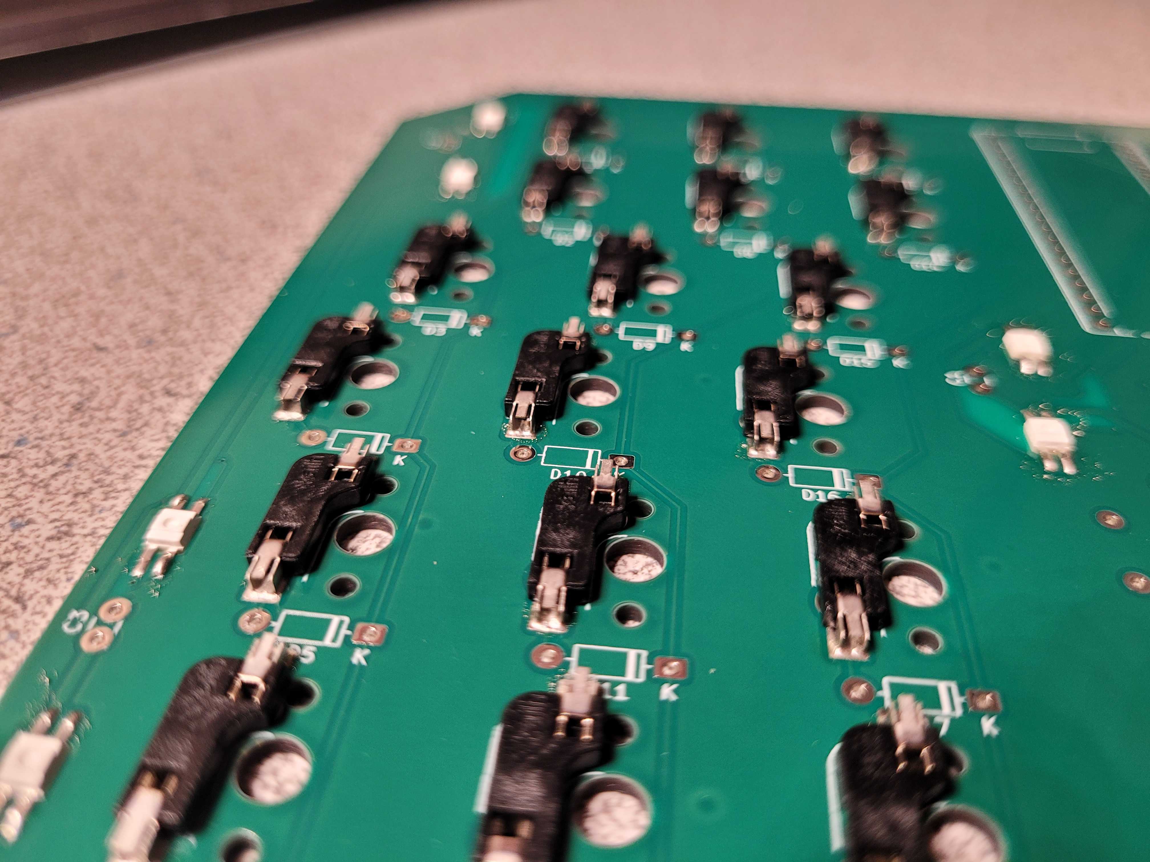
What I found really neat was how everything was magically sucked into place - even the messily pasted, half-bridged LEDs neatened themselves up. Onto the THT components!
I got everything ready and moved outside. This would hopefully go much smoother than the Hexapad with my new filament and actual flux. It did! Flux made the whole process 10x easier and quicker, and before I knew it, I was done with the diodes and joystick.
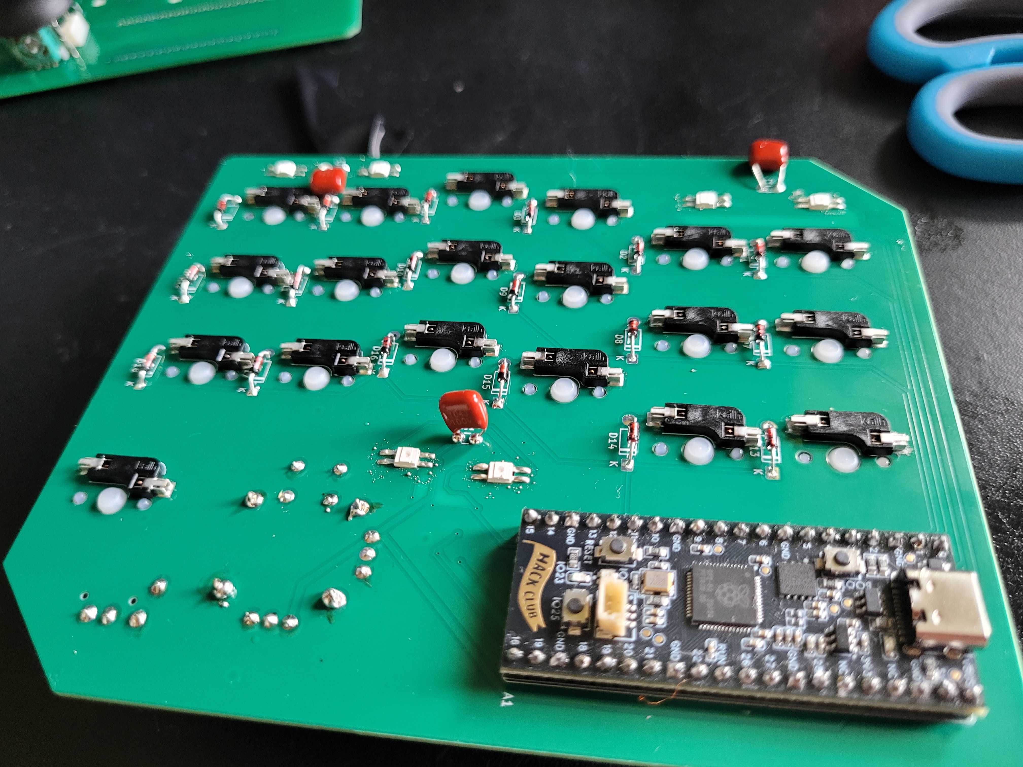
Now onto the Pico. I don't have to solder all the pins because I have some unused ones, so that cut the pad count down from 40 to 24. I had to fix a few bridges but it turned out well!
I soldered everything else on and plugged it in. It worked! Kinda. The RGB doesn't show and the bottom row doesn't work, but I'll figure that out tomorrow.
[hours worked this session: 1.5]
[total: 21]
[ JUL 25 // PROBLEMS ]
It's always a software problem.
This side of the keyboard has a strange issue: the bottom row is unresponsive and the middle row is acting as the bottom row. Even weirder, when I only scan the bottom and middle rows, the bottom row responds. So it can't be a hardware problem. I spent a bunch of time trying to figure out why this was happening, changing the code, probing with my multimeter, even trying to set up my logic analyzer. I checked the serial console one more time. When I press a key on the bottom row, I get an error about the keymap index being out of range. I disable the split module and it magically works! I think this is because I was testing with only one half.
Now to fix the RGB issues. Thankfully, this was much quicker - I was just missing some initialization code. The last thing I needed to fix was the HoldTap on the thumb button. Because I have the thumb button hooked up as a rotary encoder, I think KMK is pressing AND RELEASING the button when I press it. It looks like KMK is using tapkey() behind the scenes. I changed it to use keyboard.addkey() and added an if branch to remove_key(). This worked like a charm!
To finish today off I soldered the right side. The Pico was a little trickier this time and I had to fix a few bridges but I did manage to make it work.
That'll be all! I'm still waiting on my case and my TRRS cabe, but once those arrive I'll be able to test. See you then!
[hours worked this session: 2]
[total: 23]
[ JUL 29 // REALITY ]
Everything is here! Now I'm going to inevitably fix the firmware, then screw everything together. I put my firmware onto the right side Pico, applied some fixes so it could boot, then tried to connect them with the TRRS cable. I had to whittle some of the plastic off of the cable, but eventually made it work and connected the two sides. After re-enabling my split module, I ran into the same problem as last time: KMK was trying to press keys that didn't exist in my keymap.
In an effort to make debugging easier, I renamed the two drives to GLYPHL and GLYPHR, then got searching. It quickly became evident that I was using the split module wrong - the keymap should be exclusively on the host side. This explains all the weird errors with KMK trying to press keys that I hadn't defined. However, I quickly ran into a bigger problem - the right side kept bootlooping. It would show RGB for a split second, mount, then disappear. I tried to fix this by nuking the Pico and reinstalling my firmware, and it worked, kinda, but then my RGB dissappeared.
And then the right Pico didn't even show up as a hard drive.
[hours worked this session: 1]
[total: 24]
[ AUG 7 // OOPS ]
The Pico is fried, I think. The onboard power LED is flickering when it's plugged in. First, I tried desoldering the pico, which went about as well as you would expect:
New plan. I'm going to redo the right side. I have enough parts for a do-over - except for the joystick. But how hard can it be to find a SparkFun joystick? Spoiler: very hard. For some stupid reason someone bought literally every single COM-09032 from every single supplier and I had to find an alternative part.
I spent HOURS combing through Amazon, deciphering strange part engravings (wtf does ALPS 33 18 mean????), hunting down datasheets, and cross-referencing schematics against my CAD, trying to figure out where Sparkfun got their joysticks. I found a few amazon listings, but none of them were for sure. I eventually found the Sparkfun Deluxe Thumbstick, which is expensive but is the only option I found that I could be sure fits my PCB footprint.
Alright! That's it for today. I've placed the DigiKey order and hopefully it arrives tommorow so I can get soldering!
[hours worked this session: 2]
[total: 26]