
lumenetic-split
A split keyboard with large magnetic connectors for a charging hub featuring RGBW leds and large battery capacity.
July 4, 2025
The Background
I am starting this project with knowledge from hackpad, of making a keyboard pcb, and of making an nRF52840 circuit. Only the hackpad came to fruition, however. When I made my full-size keyboard for hackboard, I felt that I didn't have as many features as I wanted due to the part budgets so I decided not to submit it and rather use Highway to make a split keyboard. I began Highway with making an nRF52840 dev board with the same form-factor and pinout as the nice!nano, however halfway through the project, I felt that this was an unnecesarily expensive and unoriginal devboard that had already taken nearly a month.
The Keyboard
This keyboard will be a split keyboard with large magnetic connectors inspired by the Joycon 2 connectors using pogo pins to connect to a charging hub that can connect both keyboards together. It will also feature a LED bar above the keys made possible by a 18650 battery. I will also consider adding rotary encoders and a joystick. The keyboard itself will have similar layout to the ZSA Voyager.
The Microcontroller
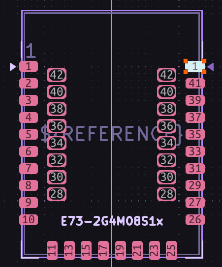
First I had to choose between the E73-2G4M08S1C and the MDBT50Q-1MV2, two nRF52840 SMD modules that were basically the same price on AliExpress and DigiKey at ~$6.


E73 on the left, MDBT50Q on the right
The MDBT50Q had only pads under it which were tiny. The E73 had castellated holes making it easier to solder, however it still had pads under it, but they were bigger than the MDBT50Q's pads. I chose the E73 because it was the easiest to solder and I can figure out a way to make them easy to solder or not use them at all.
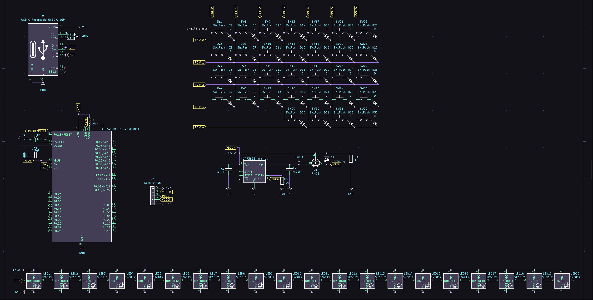
The Schematic
Given my knowledge of nRF52840 circuits after my previously attempted project, the nRF was easy to wire on the schematic as the module already came with all the decoupling capacitors (excl. VBUS), inductors, the 32MHz crystal, and the antenna. All I had to add was the VBUS capacitor and an inductor to enable DC/DC mode on REGOUT0. I omitted the 32KHz crystal because it only gives a minimal battery life boost.
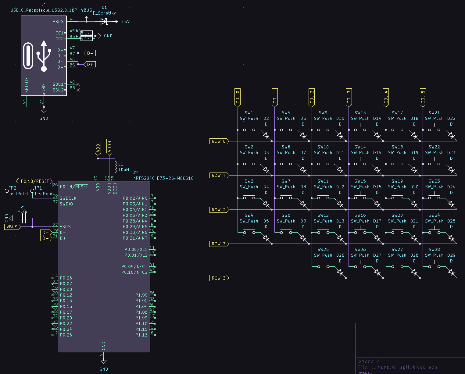
For now, I have made the matrix and USB C port on the schematic and some of the keys on the PCB.
Total time spent: 4h
July 8, 2024
This entire 2 hour session was spent on understanding 18650 batteries and finding a battery charger ic.
I did not know whether or not I needed a BMS/protection on my PCB for the 18650 battery as I thought I would be using unprotected 18650 batteries until I found out unprotected batteries are usually only used for battery packs and not small devices. Unprotected batteries lack a PCB built into the battery protecting it from overdischarge which most charger ICs do not have. I decided on using protected 18650 batteries without putting a BMS on the PCB.
Moving onto the charger IC where I spent an HOUR, I ended up choosing the BQ24072. While looking for one, I TRULY did not want to choose a Texas Instruments charger because of their datasheets. I also wanted to try and find an IC in a package with leads because I want this to be fully solderable with a soldering iron. I did find one, the LTC4000 but it was basically unsourceable or was too expensive. Landed on the BQ24072, the least complicated to wire.
Total time spent: 2h
July 11, 2025
The Charger
I wanted this to be fully solderable with a soldering iron, so I decided against using a loading sharing/powerpath battery charger IC which only come in packages with no leads. Instead, I decided to use regular battery chargers that have an IN and BAT pin, with no load sharing. To add load sharing, I searched for load sharing circuits with the TP4056 which all included a MOSFET. I then looked at a video explaining MOSFETs which had me stumped for hours. It only clicked until I watched this video.
The circuit I am using will be this one from here with a P-channel MOSFET.
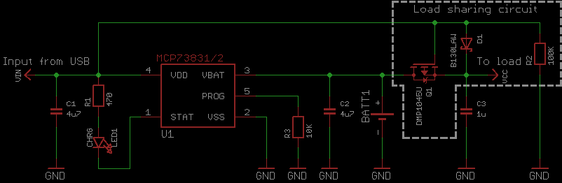
This also stumped me for hours because this was very difficult for me to understand as VBAT would be going through drain to source somehow which I didn't know was possible. I learned that it would also make VGS enough to turn on the MOSFET with this website that explains the exact same circuit.
Now another hour was spent on finding a hand-solderable IC and understanding IC packages. I was targetting a SOIC or SOP package but because of those just not existing for some reason and being too expensive when I found one, I had to settle on MSOP packages which have closer pin pitches.
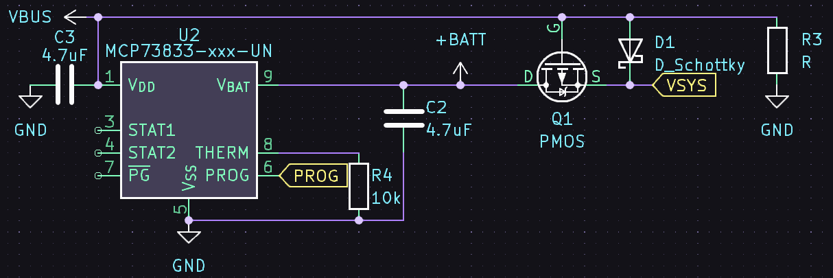
I chose the MCP73833, a 1.1A MSOP battery charger IC. I would have chosen the TP4056 but I literally couldn't find it anywhere.
The Wiring
For now this is the charging circuit. I'm unsure what to do with the STAT and PG pins, status pins that sink current for an LED or being detected by an MCU. I'll have to choose an actual MOSFET and Schottky diode which R3 depends on as well.
Total time spent: 7h
July 13, 2025
The Connector
I will be using pogo pin connectors for this which has to have atleast 5 pins.
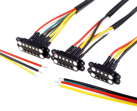
- Pins 1 and 5 will be GROUND
- Pins 2 and 4 will be 5V (VDOCK)
- Pin 3 will be PROG (explained in next section)
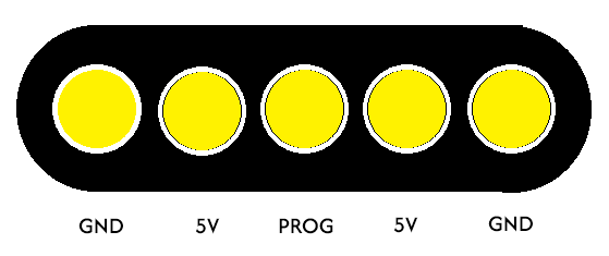
I could pass the status pins from the battery charger to the dock but that would require at least 2 more pins. The pogo pin connectors rise in cost the more pins there are.
The Dock
The dock will have an MCU module inside that can sink current through its GPIOs.
There is a problem here that can arise at any moment here: The user's charger/power supply cannot supply the current that both keyboards are demanding.
To solve this I would be passing the PROG pin from the keyboard's charger to the dock. The PROG pin controls the charger's charging current for the battery. There will be parallel resistors leading from the pin into multiple GPIOs. The MCU will communicate with a PD controller to figure out how much current to allow the chargers and sink the resistors accordingly.
The Savior
Moving onto the LDO, I nearly chose an unsuitable 3.3V without realising, the R1172H331B-T1-FE. This comment saved me by teaching me about power dissipation.
At full power, the NeoPixel LEDs I will use can draw up to 60mA each. Using the formula Power Dissipation = (Vin - Vout) * Iout, I can see that I will need at least 1530mW of power dissipation to power 30 LEDs at half power when inputting 5v through USB. I'm not sure yet that I'll use 30 LEDs nor that I'll run at them at half power but I'll be choosing another one.
This is the schematic so far. Since 70 keys is a commonly sold amount of keys, I added an extra column of keys.
Total time spent: 6h
July 14, 2025
The Lights
After looking at SK6812 RGBW LEDs, I realized that their power supply voltage has to be 3.5v-5.5v, making an LDO somewhat useless here.
There's a problem here: The 3.7v li-ion battery will operate in a range of 3.0v to 4.2v. The acceptable logic input voltage for the LEDs are -0.5 ~ VDD+0.5. When the battery is at 3.8v-4.2v, the 3.3v logic voltage of the nRF's GPIO will be out of range. That is until I saw that WS2812B LEDs work with a logic voltage of 75% of their power supply voltage, meaning 3.3v GPIOs will work when
The Design
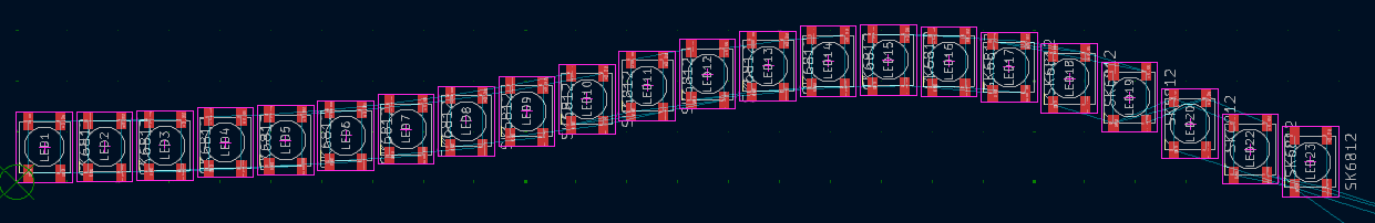
At this point, I realized my original idea for the LED bar, a straight line, was boring, so I instead tried to make it into a curve... and gave up. Here's a GIF of the attempts (i held down the redo button).
Total time spent: 4h
July 15, 2025
The Footprints
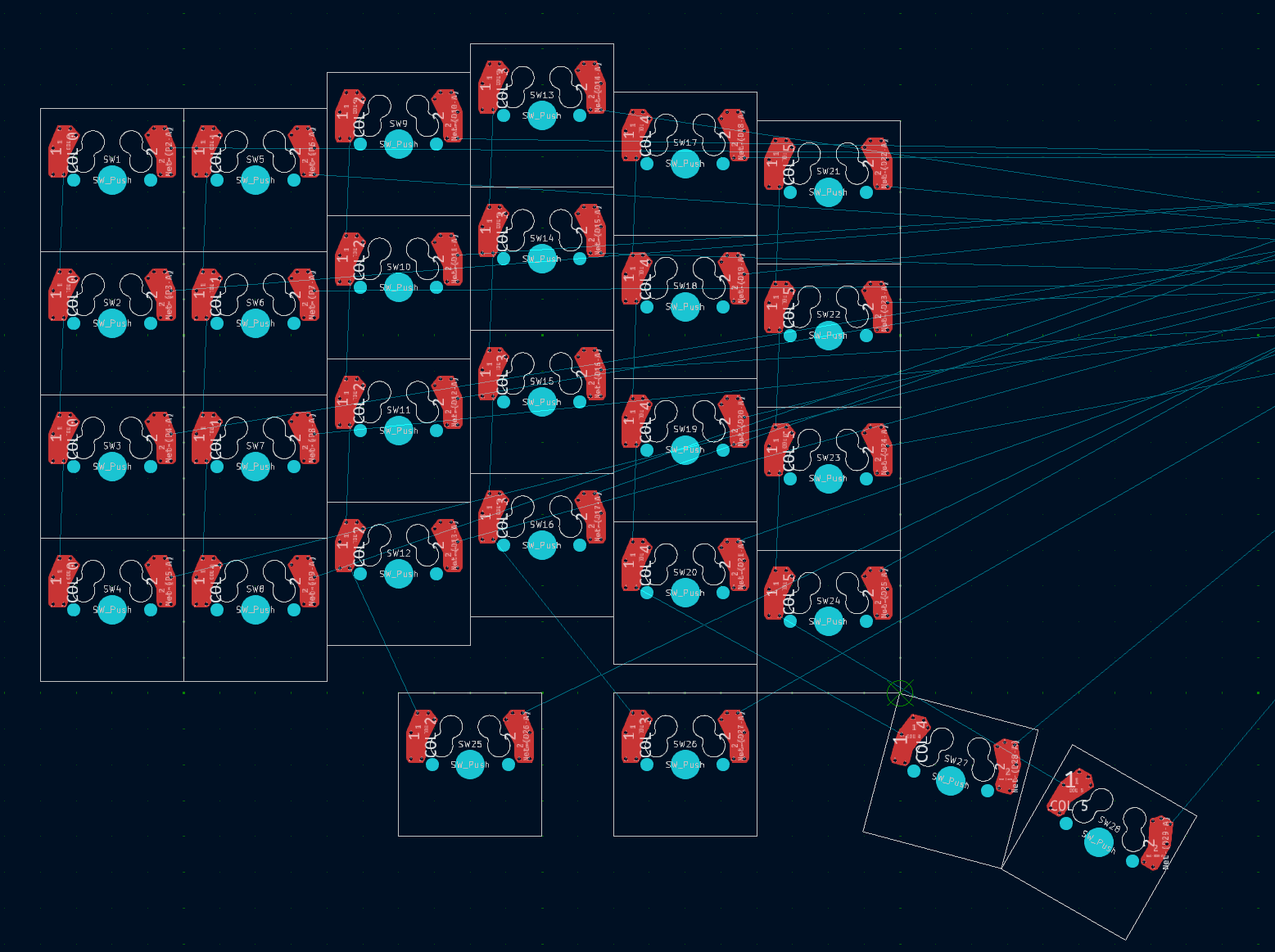
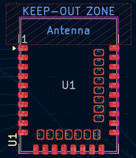
I forgot to mention that this is a reversible PCB, so it'll need reversible footprints. So far I have used reversible hotswappable MX footprints. I also made my own reversible SOD-123F footprint.
This is meant to be fully hand solderable so I made this footprint with large inner pad slots for the E73 as well.
The Curve
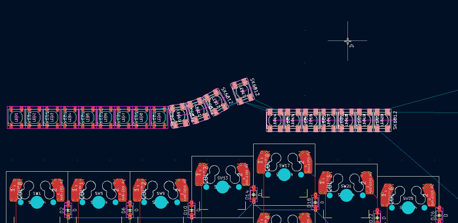
I decided to attempt making the LEDs curve again, this time with a Bezier curve. I used this Desmos template to create one where I used measurements of the MX switch bounds to align the LEDs. I then figured out where to place them just by drawing lines along the Y-axis and zoomed in to estimate because Desmos randomly decided that it didn't want to create intersection points. I messed up and restarted only 3 times, a personal record. This took me 4 hours...
Total time spent: 5h
July 21, 2025
The Logic
In solving the logic level for the LEDs, I have decided to use SKC6812 LEDs that allegedly support 3.3v logic at 5v, as seen here. The forward voltage drop of the schottky diode on the load sharing circuit will also bring the input supply voltage closer to 3.3v.
The Gate
On most microcontroller boards meant for keyboards like the nice!nano and the Supermini nRF52840, they have pin P0.13 tied to the enable pin of their 3.3v regulators. This is mostly meant for cutting power to Neopixels when they are not being used as the draw up to 1mA per LED. I integrated this ability with the same MOSFET
The Battery
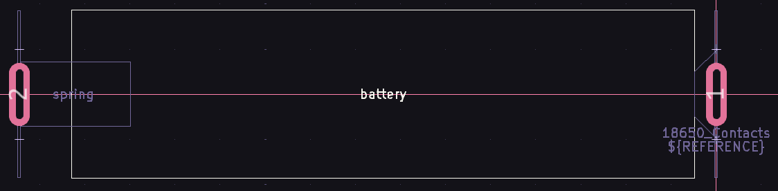
I wanted to fit the 18650 battery next to the thumb cluster, however many battery holders were simply way to large. So I made my own battery holder.
- I chose a battery, specifically this one which gave me dimensions.
- I found battery contacts on AliExpress. This one was difficult because I could not find precise measurements for battery contacts immediately but eventually found them.

- I created a footprint with a graphic of the battery and battery contacts with their dome and spring. I then lined up through hole pads where I could solder the battery contacts.
Total time spent: 5h
July 24, 2025
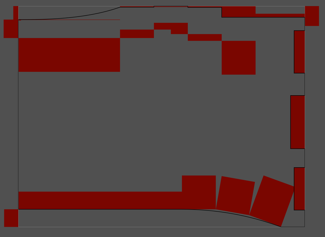
The Outline
In making the PCB outline, I had a problem with wanting the top outline to appear rectangular and not use a curve but because of the LEDs, I would have to use a curve if I didn't want the entire thing to be boxy.
I used Inkscape and very awkwardly and perfectly used recetangles to make the outline through snapping. This came out way too stupid looking and after multiple other attempts I decided that I would have to rethink the entire keyboard's layout.
With other keyboards, you can see the case follows the shape of the keys, creating a look that I like.

Example 1 source
However, the LEDs interfere with the design which means I wont be able to achieve that look. This keyboard below did change my mind though.

Example 2 source
When I remaking the column stagger, I significantly lessened the stagger in order to make the keyboard shorter.
Total time spent: 4h
July 29, 2025
The Circuitry
There are so many things to protect this keyboard's charging circuit from. I really cannot figure out how I would implement it into ZMK when I think of solutions that use I2C. So I opted to abandon the hand-solderable-with-a-soldering-iron aspect of the keyboard and to use hot plates and QFN packages.
Because I'll use QFN packages now, I can replace these hand-solderable packages with: - The entire charging circuit -> BQ24075, a variant of the charging IC I started out with - USB PD sink controller IC with low capability -> I2C USB PD sink controller (for the charging dock) - A through hole USB C port -> SMD USB C port which makes reversibility easier
The BQ24075
I realized that the connector's magnets are opposites so making the connector reversible was pointless. That means passing information between the dock and keyboard won't require as many pogo pins than being reversible. Because I'll be using the BQ24075, the charging is made easier as it is far easier to tell it how much current is available.
The (now 6) pins will be - Power - EN2 (from bq24075) - EN1 (from bq24075) - Gnd (for detection) - ILIM (from bq24075) - Gnd
Originally, I could have gone with the BQ24072 for measuring the battery but the BQ24075's SYSOFF pin would make a power switch much more easier as I wouldn't have to use an expensive high current slide switch or a low current switch with a MOSFET, both which will require large traces or large PCB copper heatsinking in an already crowded PCB. For measuring battery, I'll have to use a voltage divider, a solution used in the nRFMicro, a nice!nano alternative that uses the same E73 module.
Wiring this up was easy, only after spending a total of probably total 10 hours staring at a Texas Instruments data sheet across my previous project and this one. On the EN pins, I pulled them up and down to put it into USB500 mode at all times when not being charged by the charging dock. This is so that when standalone, it can properly and safely charge through its USB C port. When connected to the charging dock, it can change the EN pins to be able to control ILIM with a resistor. This way it avoids complicated parallel resistors with an already complicated equation.
The Blunder
I was having trouble figuring out how to route a E73 reversible footprint I made which was completely unneccesary.
Unfortunately I approached this with an even worse solution.
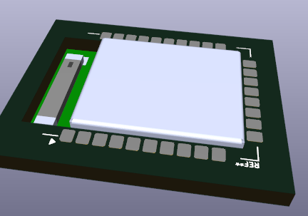
Being unable to route lines under the module wasted my time as I went back to using a normal E73 footprint which I don't know why I changed from anyways.
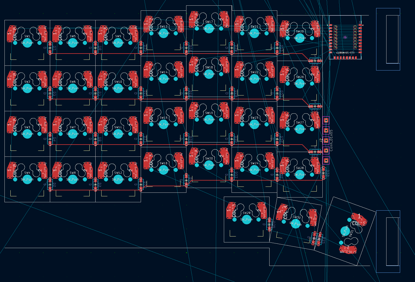
This is the PCB so far
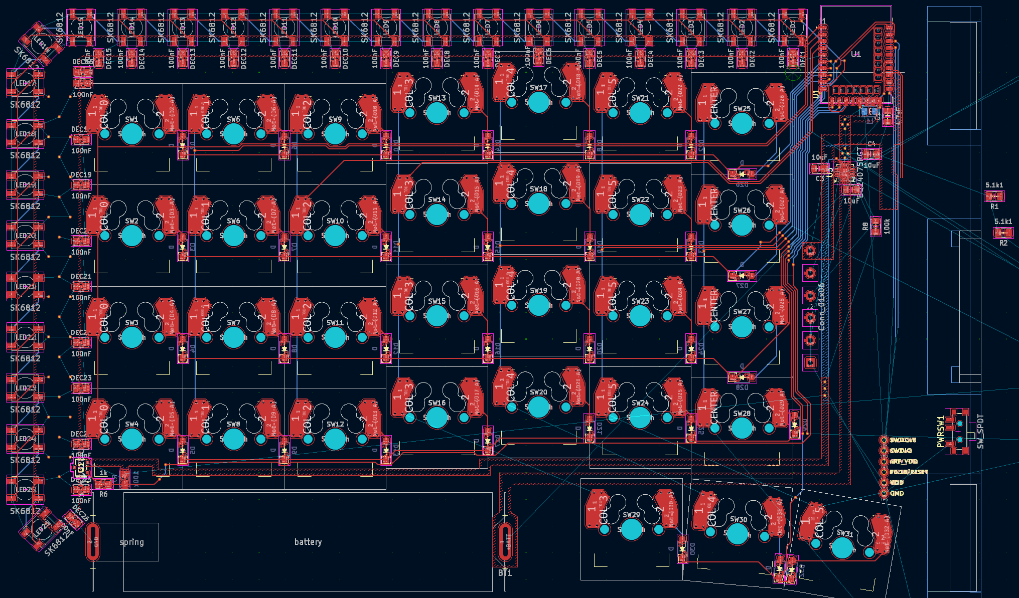
Total time spent: 8h
July 30, 2025
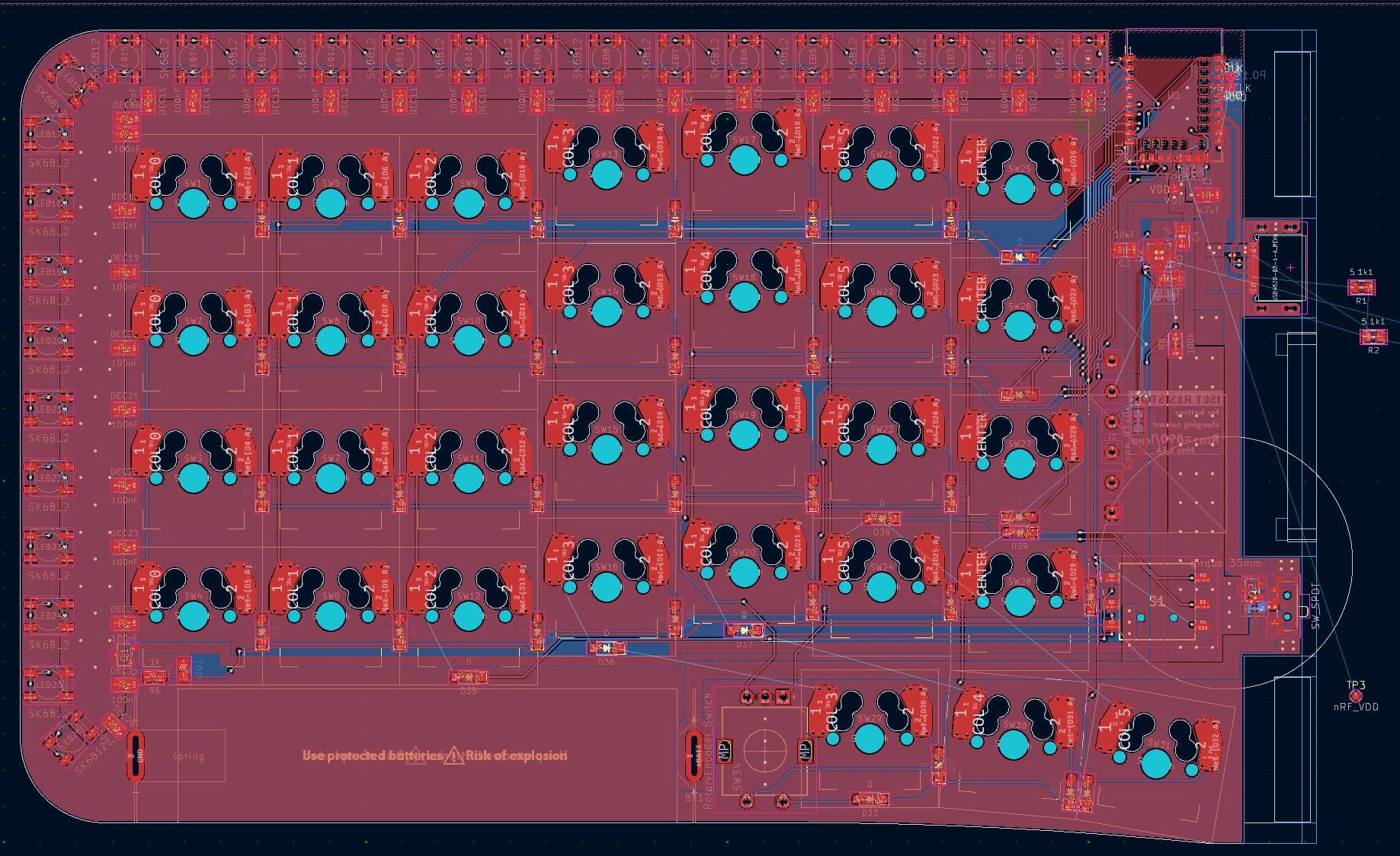
The Routing
This entire day was spent on routing this very complicated PCB. I honestly thought this was going to be easy. It is so confusing working with so many polygon fills. I also decided against the BQ24075 and went for the BQ24072 because its SYSOFF pin also disables charging and simplifying battery monitoring. With this change, I use a mosfet to toggle the output of it with a low current slide switch. I have no idea whether or not if my PCB copper heatsinks are adequete enough or too much... oh well.
I managed to squeeze in the 5-way switch and rotary encoder with horrific routing. I also want to include a 35mm cirque touchpad. I have no idea where to put the I2C pull-up resistors and pads for it. I may start using 0603 resistors.
Tomorrow I have to absolutely speedrun the charging dock, software, and case before the July 31st deadline for highway...
Total time spent: 9h