Thrust-O-Matic Mainboard
The electronics portion of Thrust-O-Matic - my rocket motor thrust stand project.
Total time spent: About 54h, +-5h because I haven’t exactly been timing it
17.6.2025 - Start of project (4h)
I have experimented in the past with KNSB rocket motors but had no reliable way of measuring their thrust. For that reason, I decided to build a thrust stand. Instead of going with the typical vertical motor orientation seen in most hobbyist solid motor thrust stands, I will use a horizontal setup. While this increases the mechanical complexity of the design, it should allow me to measure both the thrust and the weight of the motor.
I would also like to measure the chamber pressure of the motor using a pressure transducer. The thrust stand will include a wireless ignition system as well.
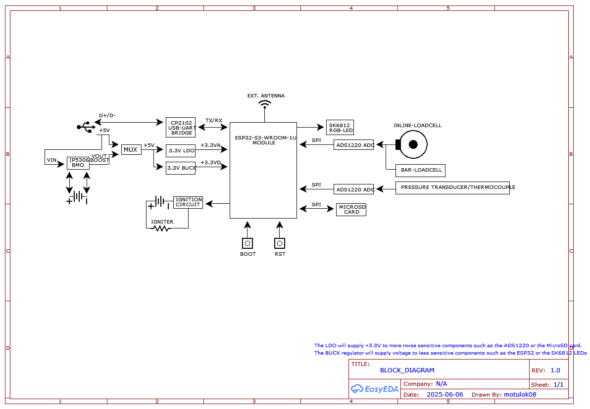
I have chosen the ESP32-S3-WROOM-1U MCU for its excellent wireless functionality, ample GPIO pins, fast processor (which should providing enough headroom for data logging, BLE, and data acquisition) and the U.FL antenna connector, which allows me to use a much more powerful antenna than the default PCB one on the standard WROOM variant.
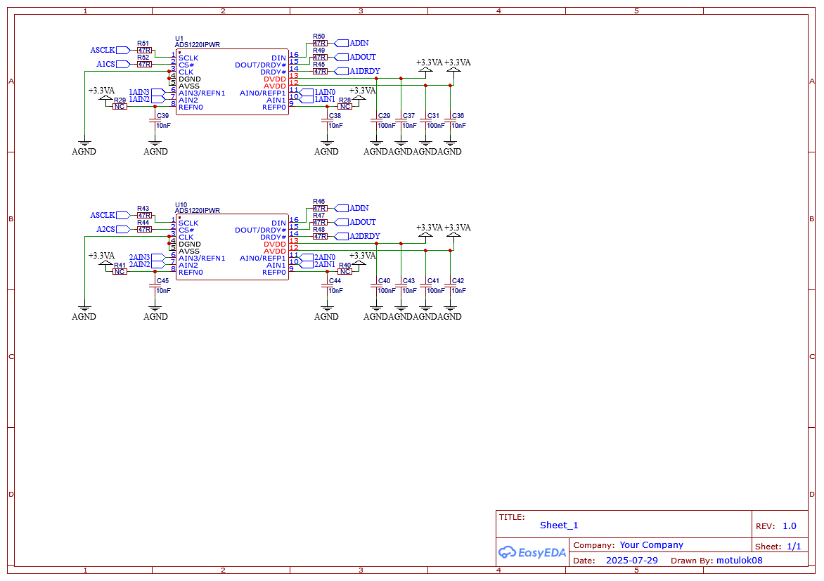
For analog-to-digital conversion from the sensors, I decided to use the ADS1220 ADC. It supports two differential inputs, allowing me to connect both the thrust and weight load cells to a single ADC and multiplex between them. This splits the sampling rate between the two channels, but that’s not a major issue since I don’t need high frequency sampling on the weight cell, as weight changes are usually slower and more linear. The plan is to sample the thrust cell at 1800 SPS and the weight cell at around 200 SPS, possibly reducing the rates if needed for accuracy.
A second ADS1220 will be used for the pressure transducer data, or potentially for thermocouple data if required.
As for the sensors, I’ve selected a generic 30 kg, 25 mm inline load cell for thrust measurement, and a 5 kg bar-type load cell for weight. For chamber pressure, I will use an XDB401 pressure transducer, which is rated for up to 5 MPa.
For the accessory ICs, I selected the CP2102 for USB-UART conversion and the IP5306 for battery management. The device will use two separate battery packs: one to power the ESP32 and other peripherals, and another dedicated to the ignition system. The main system battery will be rechargeable via USB, while the ignition battery will need to be charged separately, or possibly through a second battery charger, depending on whether I decide to integrate one.
After a couple hours of research i’ve created a block diagram of the electronics and have started work on the schematic.
Block diagram:

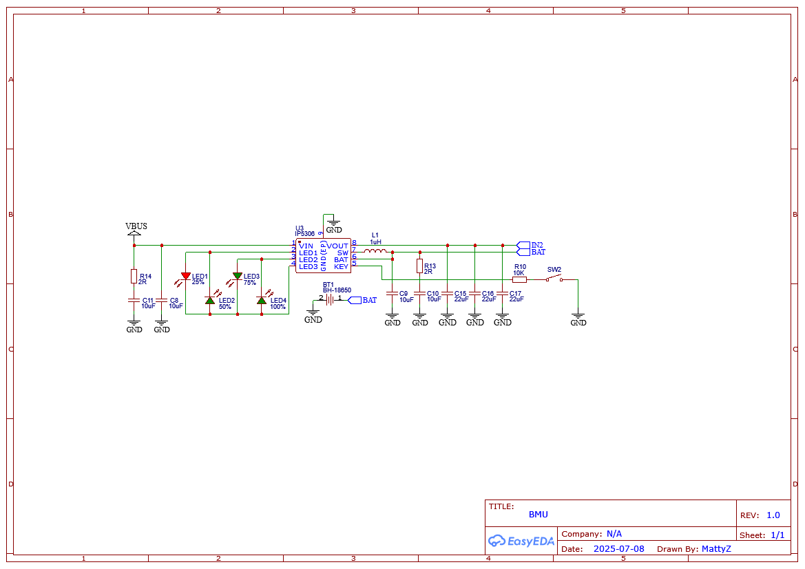
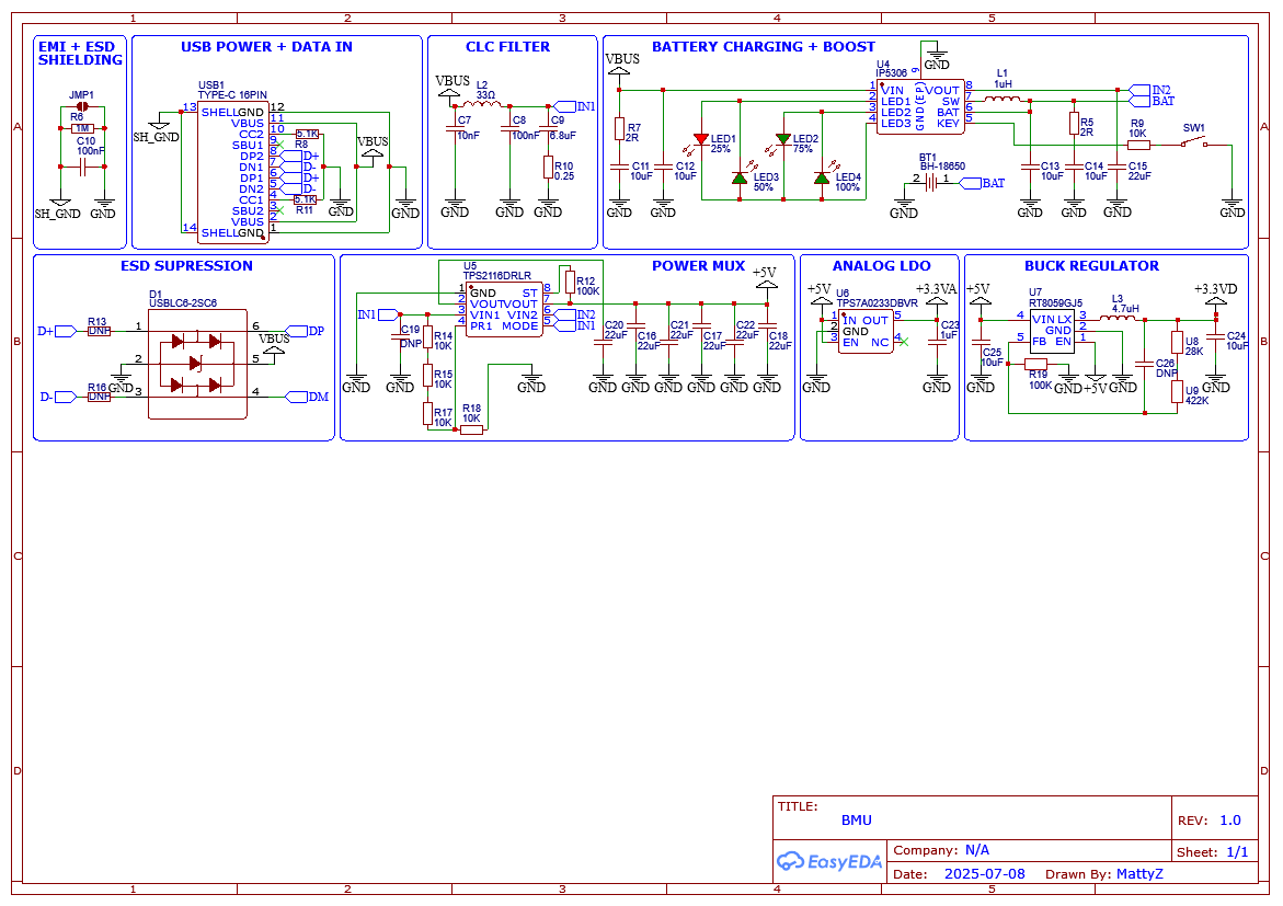
8.7.2025 - Update, finished BMU circuit (3h)
It’s been a while since the last update. I have been busy with end of the school year responsibilities and vacation. I’m currently in Poland, but I finally found some time to continue work on the project. Today, I focused on researching and drafting the schematic for the BMU.
The device is designed to charge its onboard battery when connected to USB, but only if the USB source is capable of delivering at least 3A. This functionality hasn’t been fully implemented yet. Initially, I considered using a USB-C PD controller IC to detect whether the connected USB port can supply enough current. However, I eventually decided that a simple switch would be a more simple solution. This way, the device will start to charge only when the charging is manually enabled.
The battery is necessary because the device is intended to operate outdoors where there is no access to mains power. At first, I considered using a power bank, but I eventually went for a dedicated battery instead. It also gives me a chance to better understand battery charging logic and power management.
There is not much else to say, hopefully tomorrow I will have some more time to work on the project.
BMU schematic:

24.7.2025 - Update, Block diagram revision, BMU layout changes and added USB + some protection (4h)
So today I spent a good amount of time reading datasheets and diving deeper into the power delivery side of the project. Most of my focus was on figuring out how the system should handle it’s power. After some research, I came up with what I think is a solid approach.
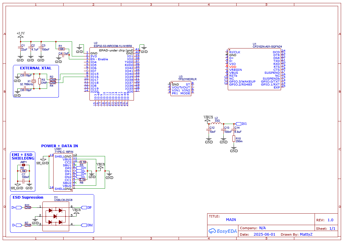
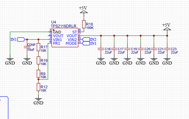
The device should draw a peak current of just under 1A, with a typical draw of around 500 mA during normal operation. This keeps it well within the range of what most USB sources can safely provide. When connected, the device will automatically switch over from battery to USB power using the TPS2116 power MUX.
It will also monitor the voltage on the USB-C CC pins and the CHR pins of the CP2102. With this information, the system can figure out the current capacity of the USB source. Based on that, it can throttle it’s current draw, by disabling power hungry components (like the RGB LEDs or radio output) or reduce the processor power if needed. If the source is capable of supplying 3A, then the VIN pin of the IP5306 will be enabled to allow battery charging, otherwise, charging is disabled to avoid overloading the power source.
I added the USB port along with a USBLC6 for ESD protection, and included EMI/ESD suppression between the USB shield and ground. I also added a simple pi filter on the VBUS line to suppress high-frequency noise.
Decided to add 2 more LEDs to the SOC indicator for better granularity. That’s about it for today. it’s been a while since the last update, mostly due to procrastination, but with the deadline approaching, I really have to pick up the pace. Tomorrow, I plan to finish up the power circuitry and also hopefully connect the CP2102.
26.7.2025 - Update, damn i did a lot of math today (3h)
Didn’t really design anything today. I was busy cleaning most of the day, but when I got back to the project, I spent a few hours going over the power system. Lots of math, checking switching times, capacitor sizing, voltage drops, thermal stuff, and making sure the damn thing will actually work. I’m about 99% confident in the design now, but you can never be sure.
27.7.2025 - Update, are you a current limiting device? Coz dam (5h)
Spent most of today figuring out how MOSFET-based inrush current limiting works and doing the math for it. Turns out my USB line has way more capacitance than the standard allows. Apparently you're not allowed to just shove whatever you want on the VBUS line, if you do so, USB will be mad at you. Also wired up the TPS2116, Nothing special.
28.7.2025 - Update, finally finished the power (8h)
Even though I spent most of yesterday trying to make inrush current limiting work, I figure that the ~28uF I have straight on the VBUS line should still be fine. Although the device isn't USB compliant, no USB source should complain about it and shut off. Since the rest of the circuit is behind the TPS2116, which does have a soft-start feature that limits current, I should be fine.
I finished up the rest of the power circuitry by adding two regulators, one linear for the ADCs and other more sensitive circuitry, and one switching for the ESP and LEDs, which shouldn’t care about voltage ripple that much. If I calculated everything correctly, I should have a voltage ripple of about 1.6mV on the buck output, which seems fine to me.
I also calculated the thermals on everything, and nothing should go above 60°C, which is also great (the only components that will actually decently heat up are the regulators). The LDO will see a max current draw of around 200mA, but normally it'll be closer to 70–90mA. The buck regulator will see a max of 700mA, but that's assuming I'm running the ESP at max compute and max broadcasting, which isn't very likely. Still, I like to calculate and design everything with plenty of wiggle room to make sure it still works even if I mess something up. Pretty good practice when designing stuff that has anything to do with rockets, in my opinion.
Even though the power circuitry took way longer than I'd like to admit, I'm pretty proud of it. Aside from the lack of inrush current limiting on the VBUS line, I think I designed it pretty well. Can’t really judge that right now though, while it might look good on paper and the calculations should add up, I won’t know for sure until I build the damn thing.
Tomorrow should be way easier, since the rest of the circuitry is pretty straightforward. With any luck, I might be able to finish the schematic, which would leave me some time to actually start the PCB layout, which is what I’m dreading right now, especially with the deadline coming up fast.
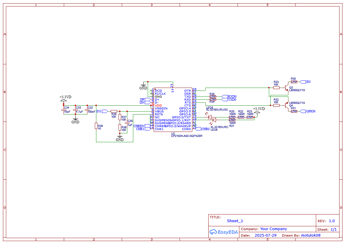
29.7.2025 - Update, CP2102N, ADS1220 connected (10h)
So today was a busy day, spent most of it working on the project. Finalized the CP2102N and ADS1220 connections in the schematic, not a whole lot to say about that. The only thing left right now is to add connectors, the ignition circuitry, microSD connections and some RGBLEDs.
30.7.2025 - Update, started routing PCB (10h)
Finally finished up the schematic and started routing the PCB, hopefully i'll finish it in time. I added the connectors, finished up the ignition circuitry, wired the microSD connector and also the RGBLEDs which I was talking about yesterday
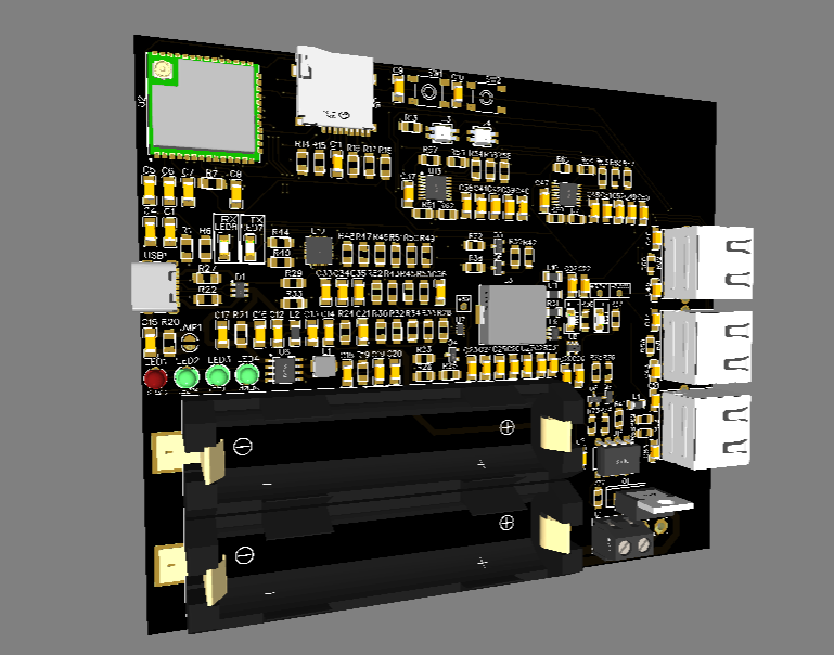
31.7.2025 - Update, finished the damn thing (12h)
Honestly im exhausted, not much to say. Routed the entire thing.