
Picoducky
Picoducky V2
What am I making?
I'm building a compact USB device based on the RP2350 Chip. The goal is to create a minimalist, plug and play board that connects directly to USB-A ports and acts as a HID device, or a FIDO security key (using PicoFido). This is the second iteration of the project. Version 1 used a RP2040 and worked well overall, but there were a few issues, like the buttons being too small and hard to press without using your nails, and the board slipping out of the usb board (Not really a design fault, I ordered 1.6mm thick pcb to save on cost for the first prototype).
My Goals For This Project
RP2350 MCU
Same Size As Version 1
Bigger Buttons
Plugs In Directly (2.0mm Thickness)
Cool silkscreen art
Total Time Spent: 13 Hours
25th May - Schematic And Rough PCB Layout
Since I already made a board using a RP2040, remaking it using a RP2350 wasn't that difficult. There were a few new things I had to take into consideration like a new circuit for the voltage regulator but other wise it was mostly the same. RP2350 Hardware Design Guide
Now for this version I decided to spend more time on finding cheap components that were in JLCPCB's basic library. This probably took more time than making the actual schematic, but in the end the BOM was a lot more optimized than V1, I did decide to not switch out the inductor for a cheaper one because the RP2350 guide suggested it worked best with those ones. For its ldo I went with the one the guide recommended which supplies around 1A and for the flash I also went with what the guide suggested but I just used the 8mb version instead of the 16mb.
After this I moved onto designing the PCB, I usually start by making a very rough layout of where the components will be to get a rough estimate of how much space its gonna take.
Layout Version 1 : The board was around 3 mm wider in order to fit the new voltage regulator circuitry.

I did not like Version 1 of the layout because it had a larger footprint than PicoDuckyV1. Plus there was a lot of empty space on the board meaning this all could be compressed down into the original footprint of the V1 (15x30mm).
Layout Version 2 : Starting to look more like what I want

I flipped the RP2350 90 Degrees counterclockwise and now everything fits nicely into the footprint of the original board (15x30mm). Also switched out the places of ldo and flash storage.
Time Spent: 6 Hours
26th May - Initial Routing
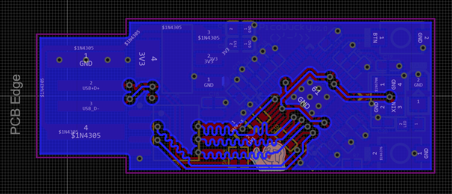
Started routing the board today. I first start off with the flash traces because I had to length tune them and ensure they were all almost the same length which took A LOT of time !!! . This was a major improvement over Version 1 of the PicoDucky which had its trace lengths mismatched by a lot (~20mm). The Data pins were also routed as a differential pair and were almost the same length.
Flash Traces

More Routing

Time Spent: 2 Hours
27th May - Routing and Silkscreen
Finished Routing all the traces. It was a pretty boring process but here are the results.
Finished Routing
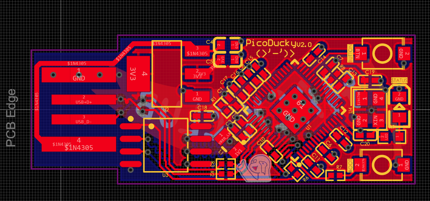
Also added some multicolored silkscreen!!


Time Spent: 3 Hours
May 29 - Improvements
I was using the AMS1117-3.3 as the LDO which provides up to 1A of current but also takes up a lot of space on the board. Since I don't have any GPIO pins on the board, supplying 1A would be pretty overkill and useless. My plan is to use a smaller LDO which can provide up to 500mA and then also add a ESD protection diode.


After switching to a smaller LDO I feel like there is too much free space on the board, I'm contemplating switch back to the SOT-23 package for the LDO.