
Hackpack
Total time: 21hrs 30m
Final notes:
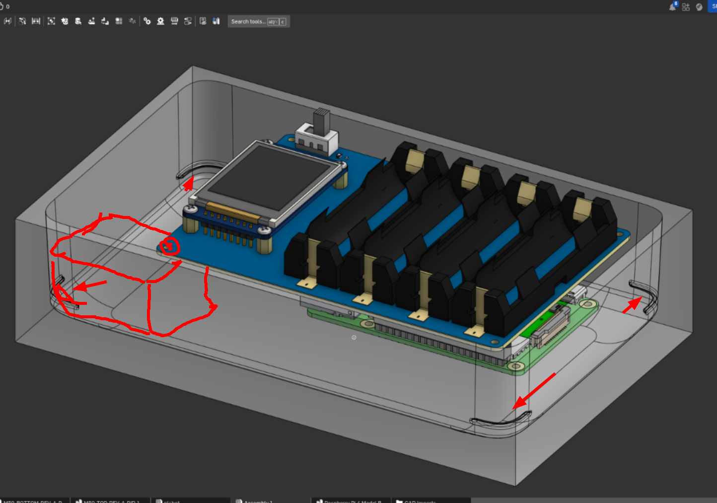
CAD couldn't prepare me for every design issue I ran in to at the integration hell
stage. There are a lot of minor design flaws, and I've learned a LOT. Stay tuned, I may give this a second shot, with the goal of perfecting this project (never gonna happen, but it's a good goal to aspire to).
August 2:
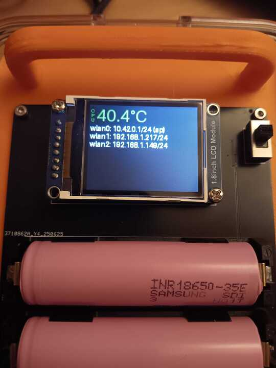
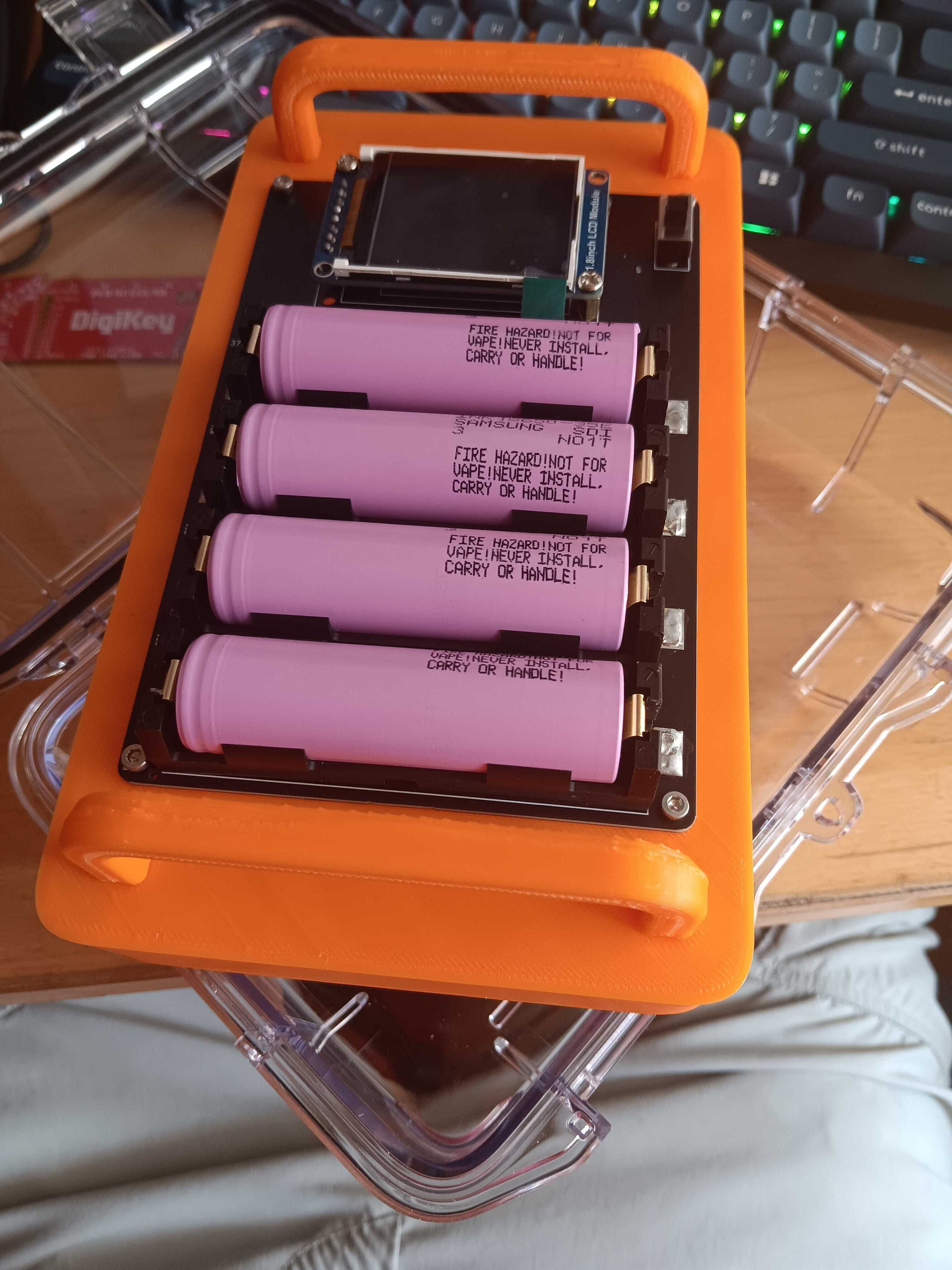
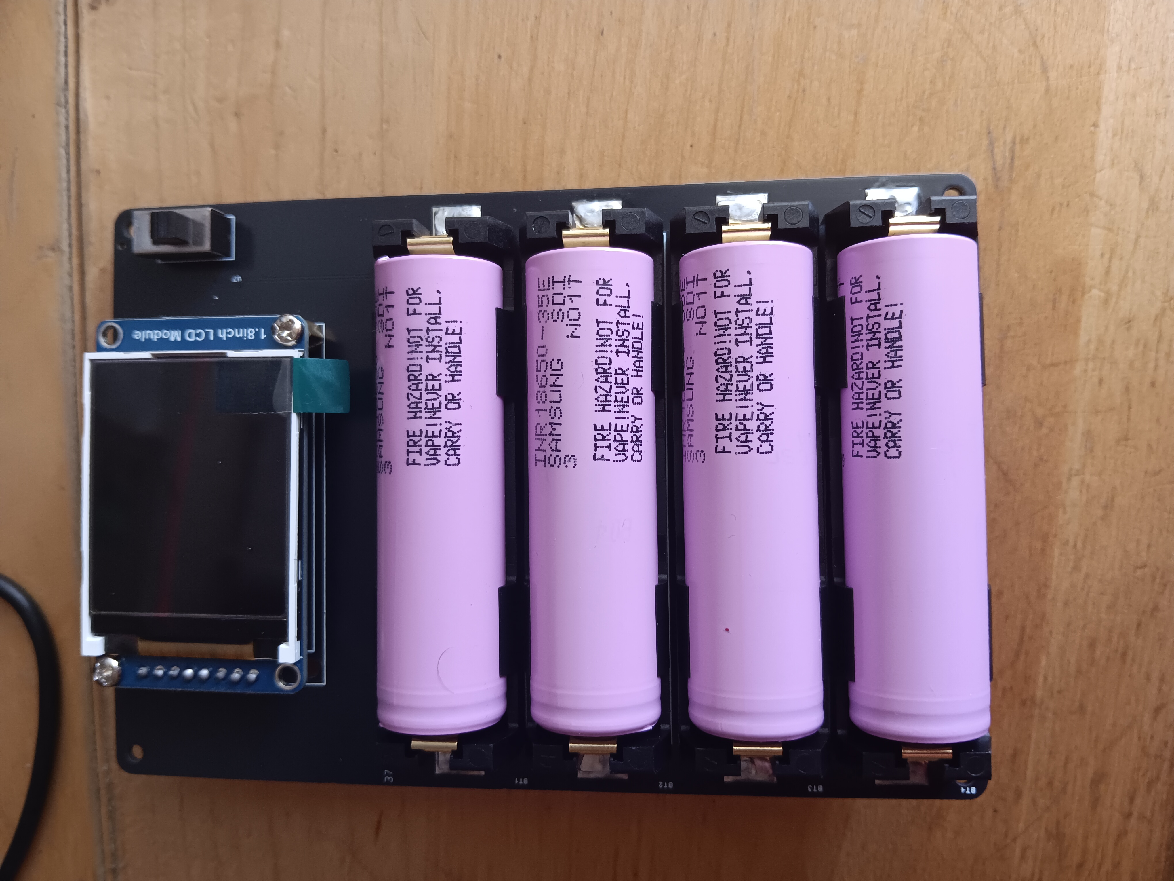
Did a bunch of work on the display, and it fully works now, so...
July 22:
Project complete!
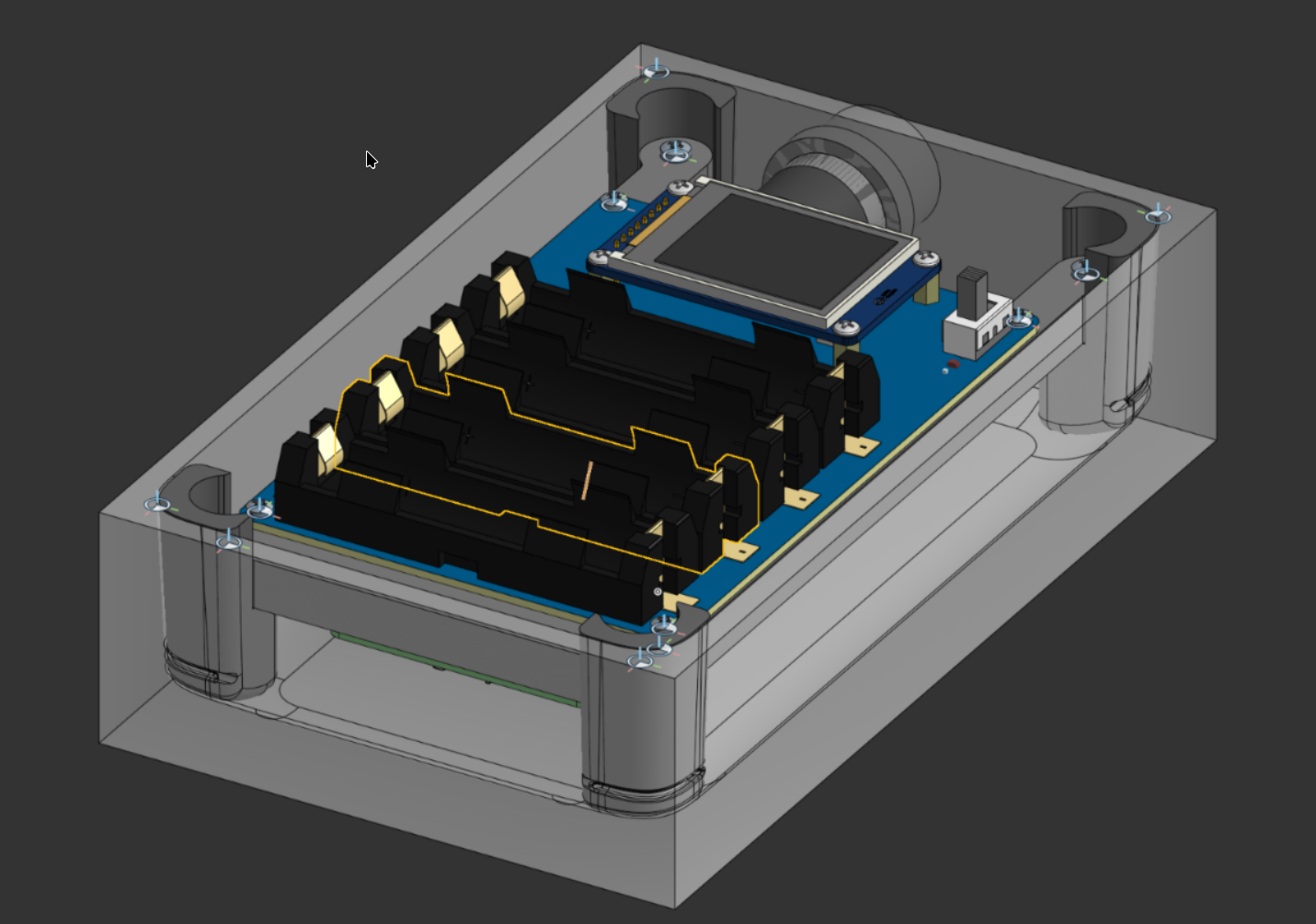
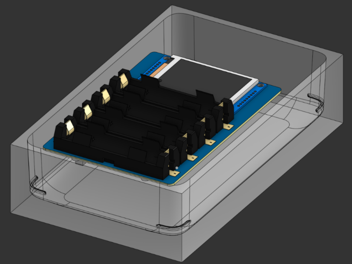
I iterated the case mount several times over the past few days, and finally got it to a place where I like it:
July 15:
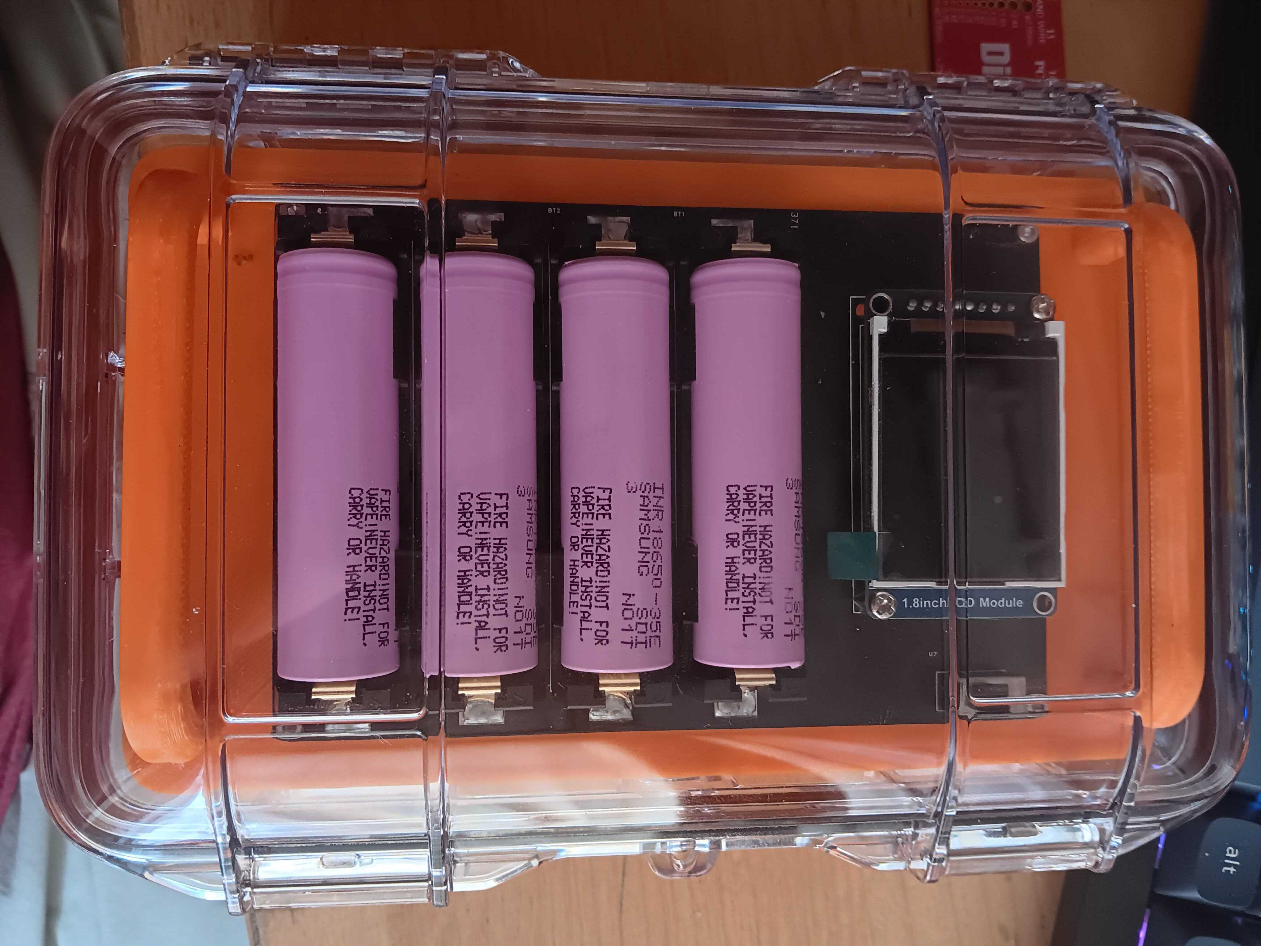
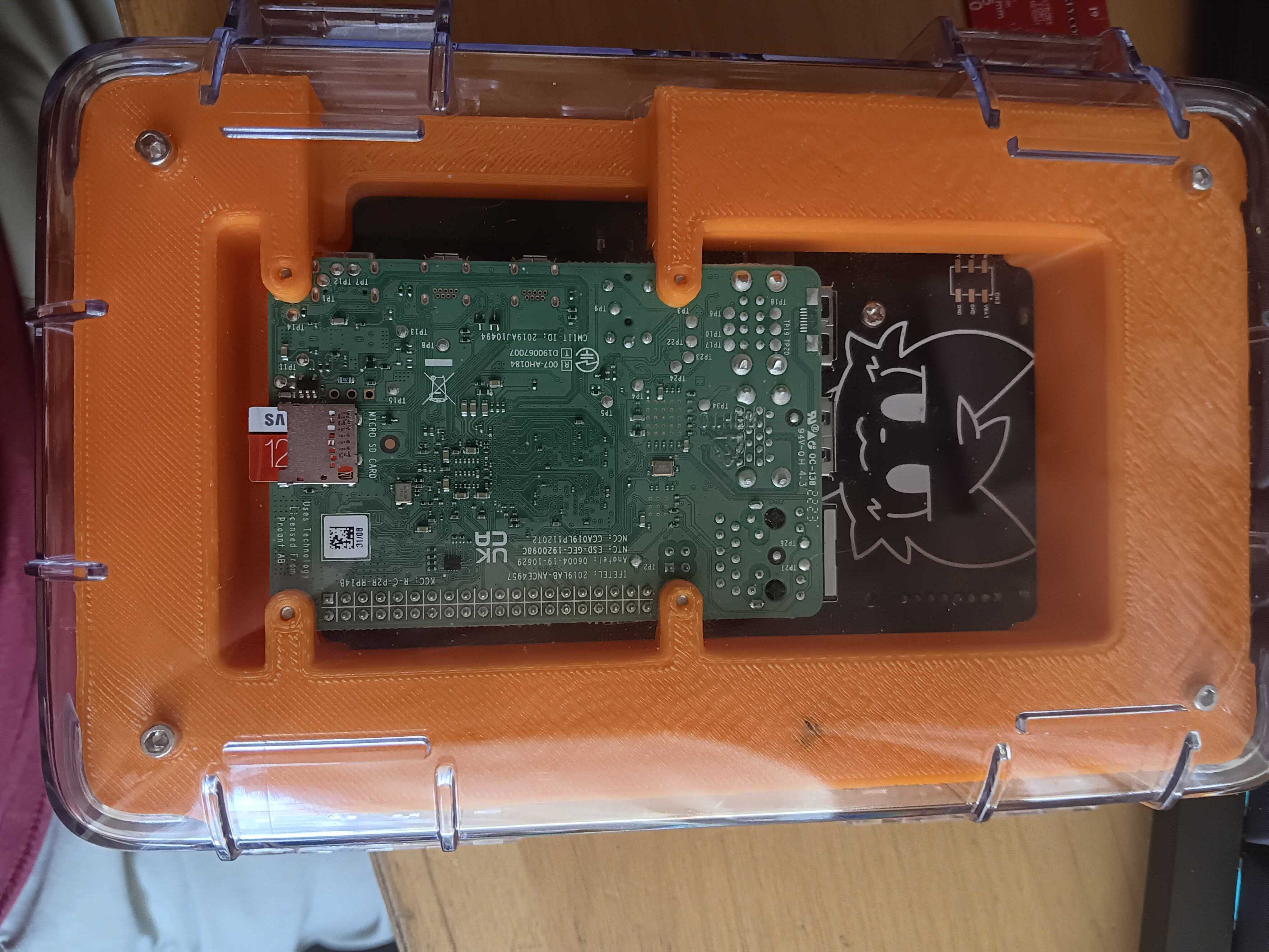
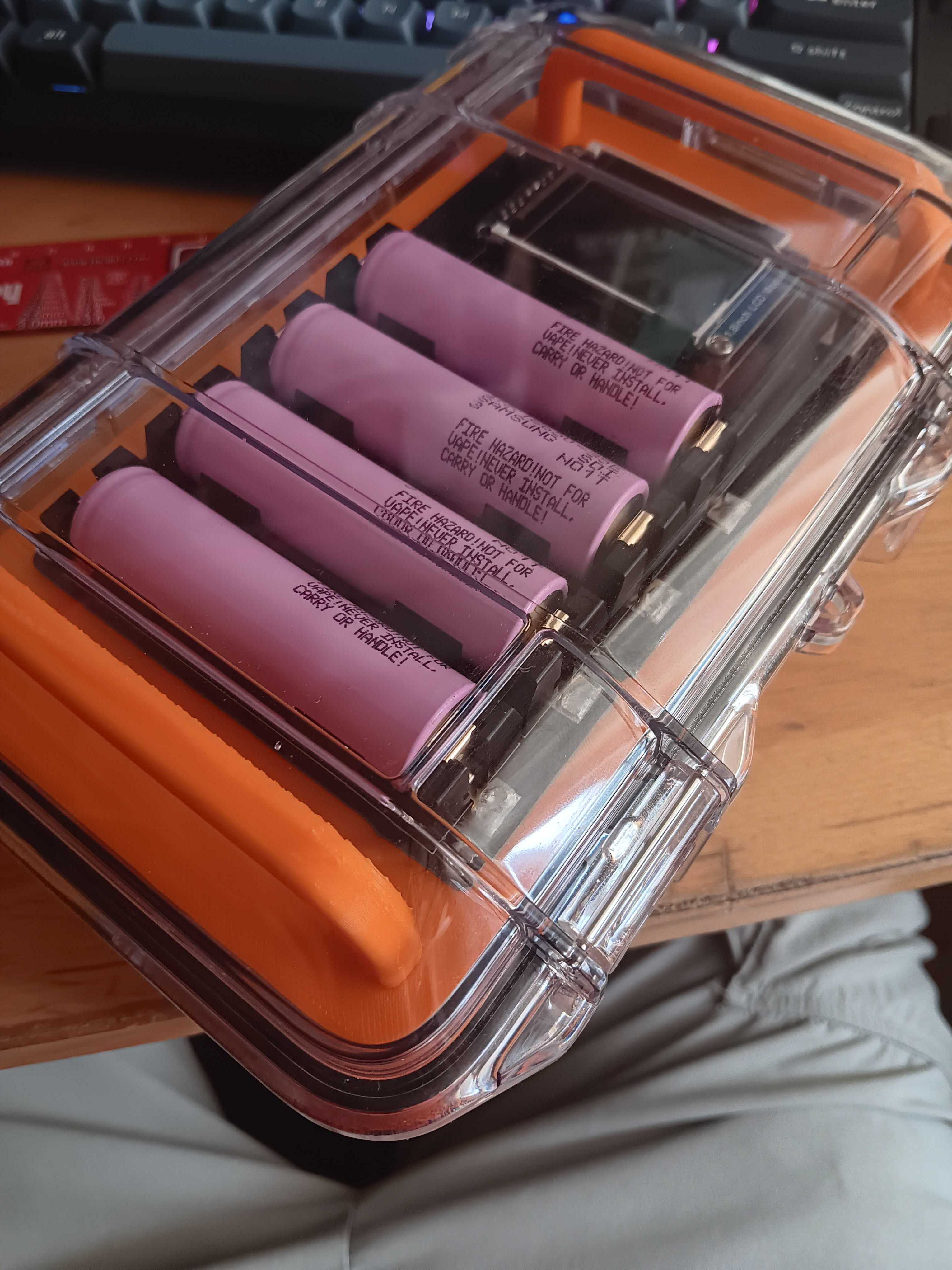
All the parts have finally arrived, and I'm back from undercity! I just finished soldering everything together, though I think I might redo the standoffs for the screen with a custom 3d print. I tested the hat, and it seems I got lucky, It's outputting 5.25v which is just on the edge of the Pi's 4.75-5.25v acceptable range.
June 24:
30m
Ordered parts after a ton of struggling with JLCPCB's website!
June 14:
2hrs
Today is mainly preparing to submit since I'm leaving for vacation tomorrow. JLCPCB's website is still refusing to works, so I might not have a good quote on the PCBs. I cleaned up the repo, made final changes to the PCB and CAD, and went over all the guidelines. Also made some relatively minor cad changes.
June 13:
4hrs
JLCPCB's website FUCKING SUCKS
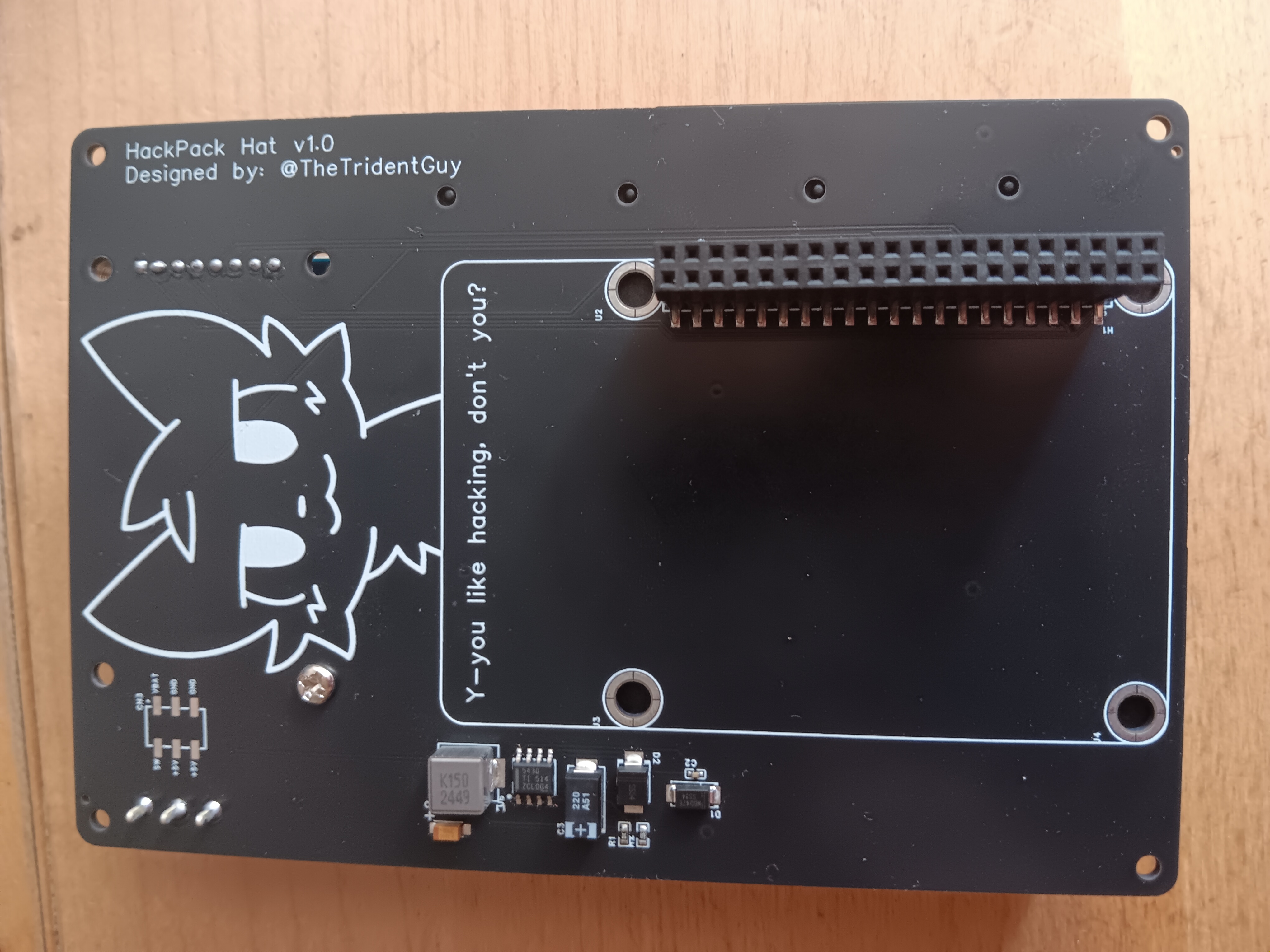
In the very real case that PCB assembly gets pricey, my contingency plan is to solder the top myself. Also added RJ45 passthrough in CAD:
June 12:
5hrs
Also put in screws, etc:
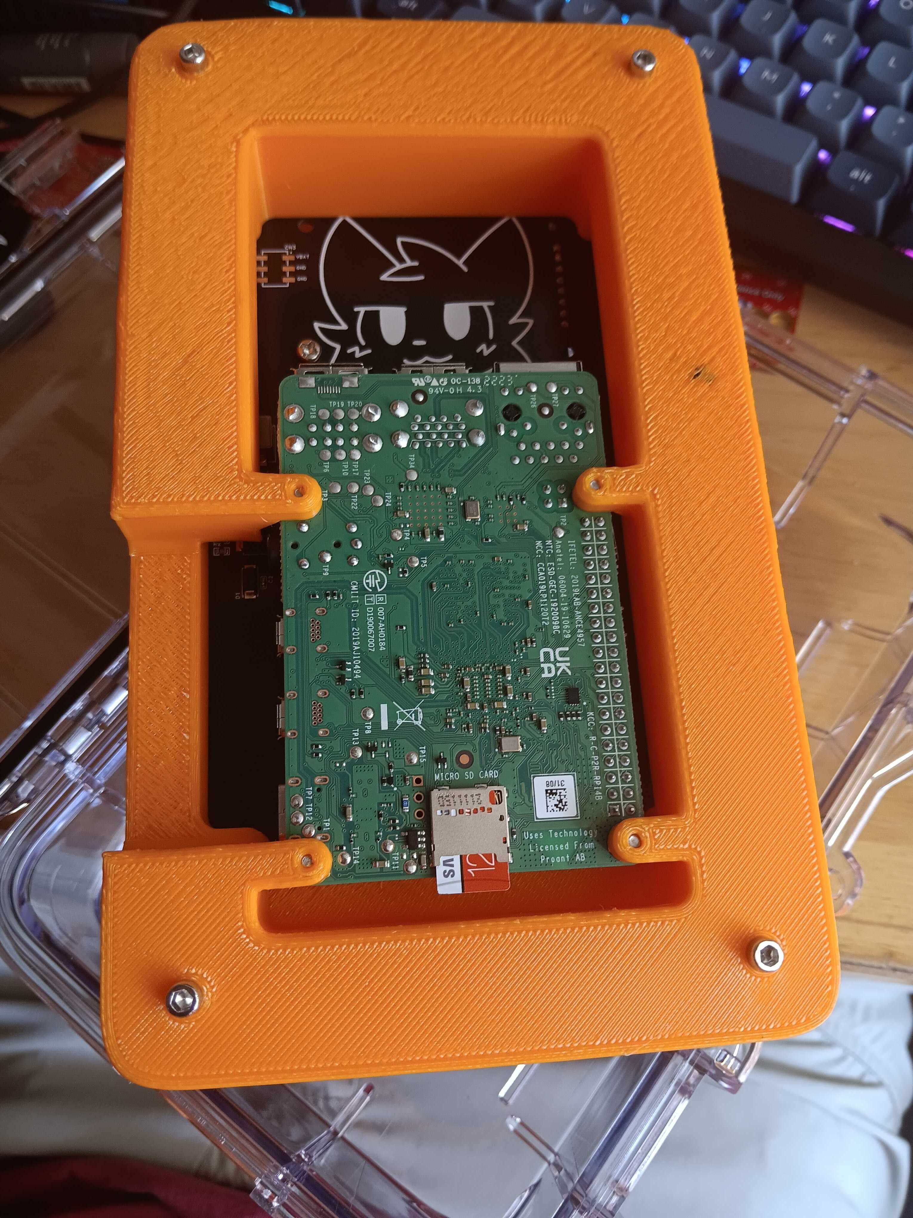
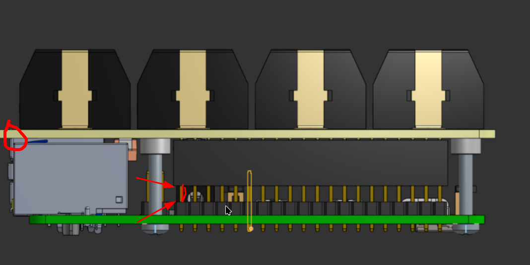
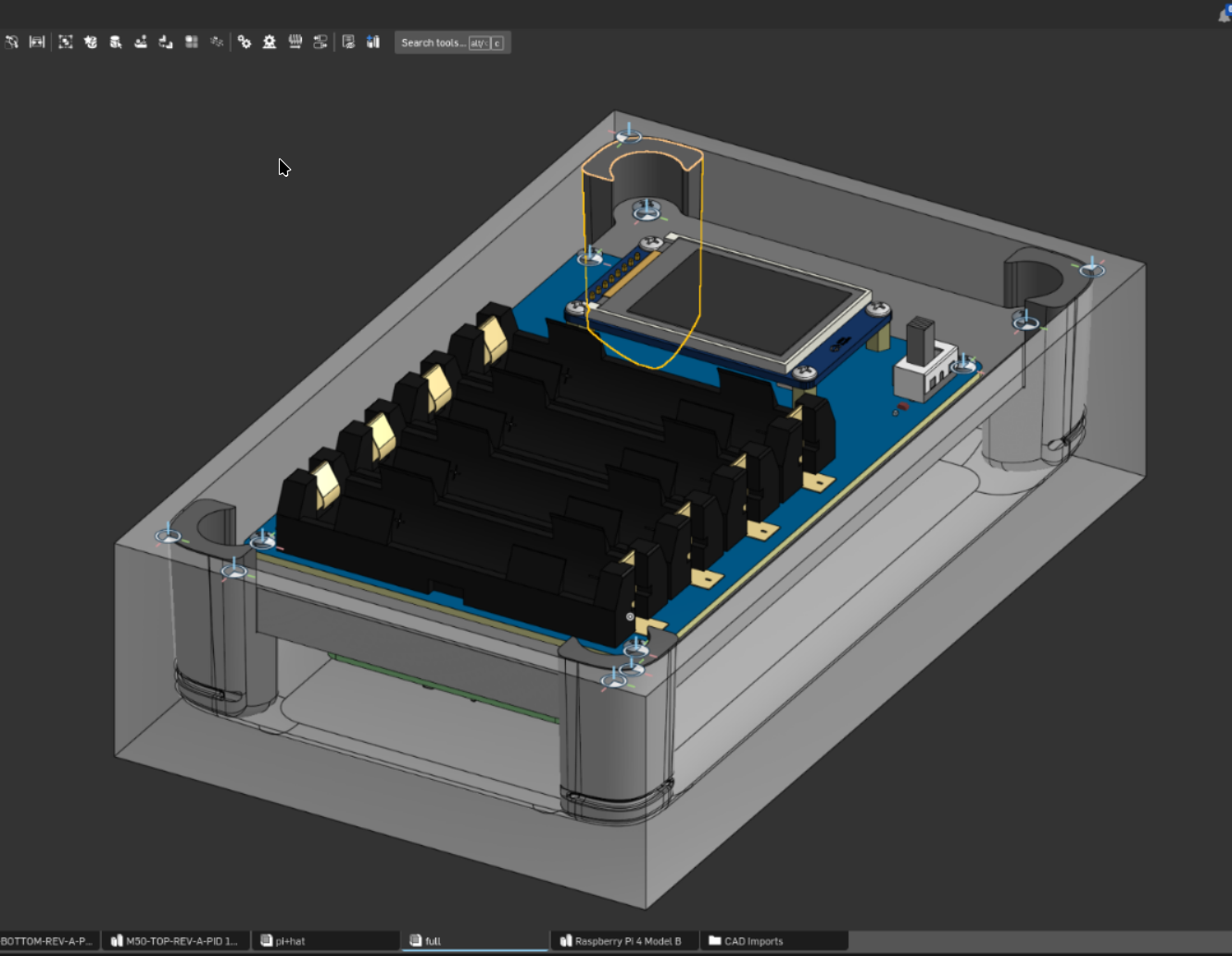 Took an eternity, but I finally figured out how to mount the board in there!
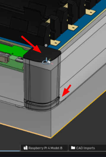
Today I'm back in CAD. it took me forever, and quite a few revisions, but i finally got these things that will eventually support the pi kinda working, and properly mating, The ridges were a massive pain, even though they're key to my design:
June 11:
5 hrs
oh and i have no idea how to mount the board in the case, im thinking something like what i have drawn below, i want to make use of the existing ribs to support the pcb:
 ALL HAIL OUR LORD AND SAVIOR: https://lcsc.com/product-detail/image/FH-00205_C2685098.html:
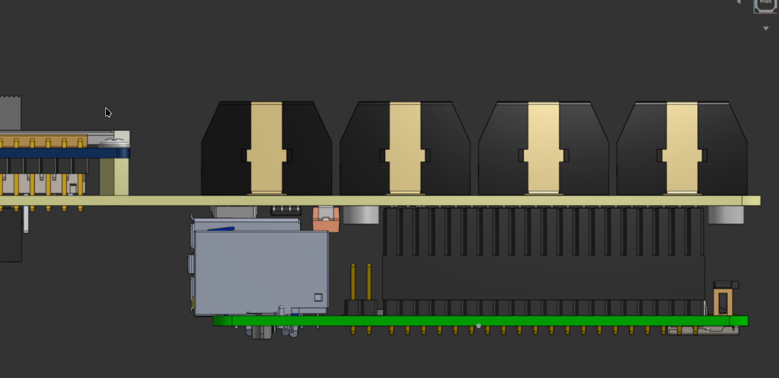
Back in CAD today, and while mocking up witrh a Pi, I realized that the header I'm using isn't quite tall enough, so I'm going to have to replace it:
 (if you zoom in you'll se that the USB ports is clipping into the PCB)
June 8:
1 hr
Copied in my power circuit from my previous trail project and got it layed out. Pic coming soon.
June 7:
2hr
v1 of pcb layout is complete! put it in cad and now have a good basic mockup:
June 6:
1hr
fuck around in cad/easyeda
June 5:
2hrs
Started planning out my PCB in EasyEDA Pro, and I am now legitimately shocked how much of a struggle I can turn placing a single pin header into pf.
June 4:
School is finally out, so I now actually have time to get some work done. I previously started a CAD document, and now I finally linked it in this repo.
May 19:
Set up basic repo, etc, also ordered some test components off of amazon.